2SD250A Overview
Description
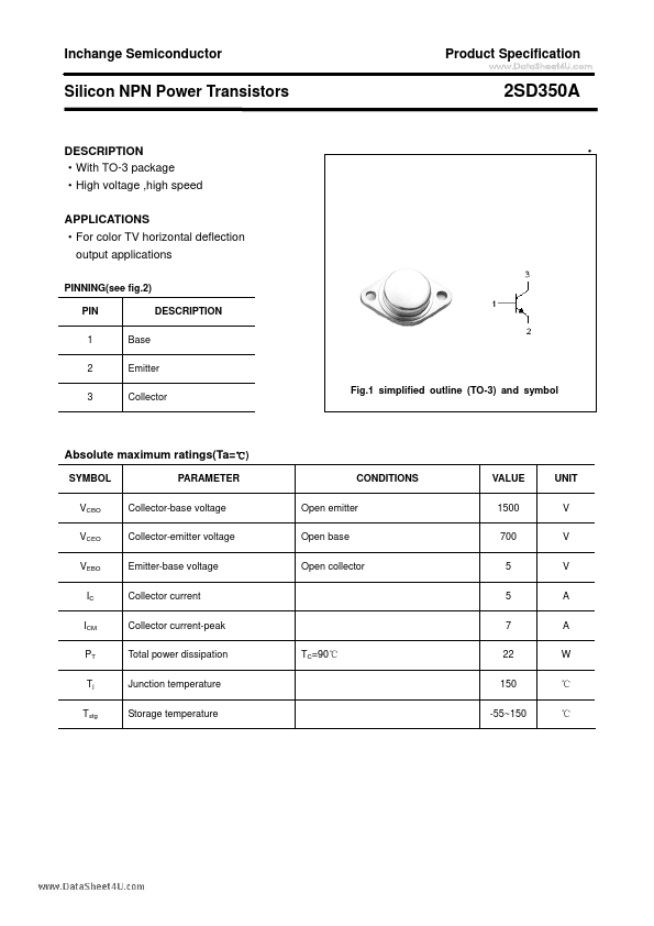
With TO-3 package - High voltage ,high speed APPLICATIONS - For color TV horizontal deflection output applications PINNING(see fig.2) PIN 1 2 3 Base Emitter Collector Fig.1 simplified outline (TO-3) and symbol DESCRIPTION - SYMBOL VCBO VCEO VEBO IC ICM PT Tj Tstg PARAMETER Collector-base voltage Collector-emitter voltage Emitter-base voltage Collector current Collector current-peak Total power dissipation Junction temperature Storage temperature TC=90℃ CONDITIONS Open emitter Open base Open collector VALUE 1500 700 5 5 7 22 150 -55~150 UNIT V V V A A W ℃ ℃ Inchange Semiconductor Product Specification Silicon NPN Power Transistors 2SD350A CHARACTERISTICS Tj=25℃ unless otherwise specified SYMBOL PARAMETER CONDITIONS MIN TYP. MAX UNIT VCEO(SUS) Collector-emitter sustaining voltage IC=0.1A; IB=0 700 V V(BR)EBO Emitter-base breakdown votage IE=10mA; IC=0 5 V VCEsat Collector-emitter saturation voltage IC=4.5 A;IB=2A 1.0 V VBEsat Base-emitter saturation voltage IC=4.5 A;IB=2A 1.3 V μA ICBO Collector cut-off current VCB=800V;IE=0 10 hFE-1 DC current gain IC=1A ; VCE=5V 8 hFE-2 DC current gain IC=4A ; VCE=10V 3 2 Inchange Semiconductor Product Specification Silicon NPN Power Transistors PACKAGE OUTLINE 2SD350A Fig.2 Outline dimensions 3.