TLE9271QXV33 Overview
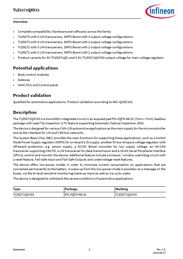
The TLE9271QXV33 is a monolithic integrated circuit in an exposed pad PG-VQFN-48-31 (7mm x 7mm) leadless package with Lead Tip Inspection (LTI).
TLE9271QXV33 Key Features
- Very low quiescent current consumption in SBC Stop and Sleep Mode
- Periodic Cyclic Wake in SBC Normal and Stop Mode
- SMPS 750mA (DC/DC buck) voltage regulator 3.3V to supply high current load with high efficiency
- DC/DC Boost converter for low battery supply voltage
- Low-Drop Voltage Regulator 5V/100mA, protected for off-board usage
- High-Speed CAN Transceiver
- fully pliant to ISO11898-2:2016
- supporting CAN FD munication up to 5Mbps
- Up to 2 LIN Transceivers LIN2.2, SAE J2602 with programmable TXD timeout feature and LIN Flash Mode
- pliant with “Hardware Requirements for LIN, CAN and FlexRay Interfaces in Automotive
TLE9271QXV33 Applications
- One universal High-Voltage Wake Input for voltage level monitoring


