BSP322P
BSP322P is Small Signal Transistor manufactured by Infineon.
..
SIPMOS® Small-Signal-Transistor
Features
- P-Channel
- Enhancement mode
- Logic level
- Avalanche rated
- Pb-free lead plating; Ro HS pliant
Product Summary V DS R DS(on),max ID -100 800 -1 V mΩ A
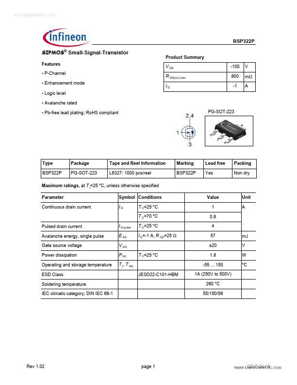
PG-SOT-223
Type BSP322P
Package PG-SOT-223
Tape and Reel Information L6327: 1000 pcs/reel
Marking BSP322P
Lead free Yes
Packing Non dry
Maximum ratings, at T j=25 °C, unless otherwise specified Parameter Continuous drain current Symbol Conditions ID T C=25 °C T C=70 °C Pulsed drain current Avalanche energy, single pulse Gate source voltage Power dissipation Operating and storage temperature ESD Class Soldering temperature IEC climatic category; DIN IEC 68-1 I D,pulse E AS V GS P tot T j, T stg JESD22-C101-HBM T C=25 °C T C=25 °C I D=-1 A, R GS=25 Ω Value 1 0.8 4 57 ±20 1.8 -55 ... 150 1A (250V to 500V) 260 °C 55/150/56 m J V W °C Unit A
Rev 1.02 page 1
2007-04-10
..
Parameter Symbol Conditions min. Thermal characteristics Thermal resistance, junction
- ambient R th JA minimal footprint, steady state 6 cm2 cooling area1), steady state Electrical characteristics, at T j=25 °C, unless otherwise specified Static characteristics Drain-source breakdown voltage Gate threshold voltage Zero gate voltage drain current V (BR)DSS V GS=0 V, I D=-250 µA V GS(th) I DSS V DS=V GS,I D=-380 µA V DS=-100 V, V GS=0 V, T j=25 °C V DS=-100 V, V GS=0 V, T j=150 °C Gate-source leakage current Drain-source on-state resistance I GSS R DS(on) V GS=-20 V, V DS=0 V V GS=-10 V, I D=-1 A V GS=-4.5 V, I D=-0.93 A Transconductance g fs |V DS|>2|I D|R DS(on)max, I D=-0.8 A -100 -2.0 -1.5 -0.1 -1.0 -1 µA V 115 K/W Values typ. max. Unit
- -
- -10 -10 600 808
-100 -100 800 1000 n A mΩ
- S
1) 2 Device on 40 mm x 40 mm x 1.5 mm epoxy PCB FR4 with 6 cm (one layer, 70 µm thick) copper area for drain connection. PCB is vertical in still air.
Rev 1.02 page 2
2007-04-10
.....