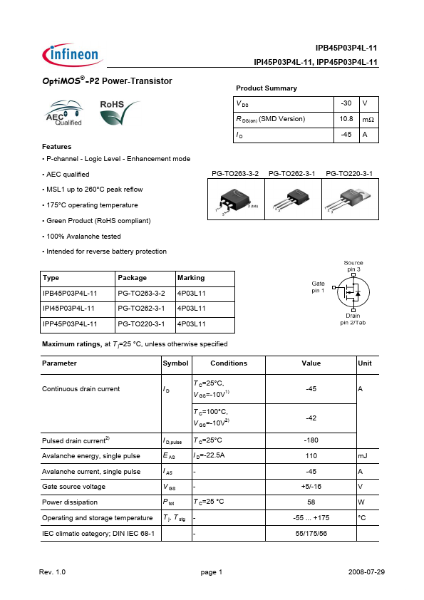
• Part: IPB45P03P4L-11
  • Description: OptiMOS-P2 Power-Transistor
  • Category: Transistor
  • Manufacturer: Infineon
  • Size: 233.56 KB
Download IPB45P03P4L-11 Datasheet PDF
Infineon
IPB45P03P4L-11
IPB45P03P4L-11 is OptiMOS-P2 Power-Transistor manufactured by Infineon.
.Data Sheet.co.kr IPB45P03P4L-11 IPI45P03P4L-11, IPP45P03P4L-11 Opti MOS®-P2 Power-Transistor Product Summary V DS R DS(on) (SMD Version) ID -30 10.8 -45 V mΩ A Features - P-channel - Logic Level - Enhancement mode - AEC qualified - MSL1 up to 260°C peak reflow - 175°C operating temperature - Green Product (Ro HS pliant) - 100% Avalanche tested - Intended for reverse battery protection PG-TO263-3-2 PG-TO262-3-1 PG-TO220-3-1 Type IPB45P03P4L-11 IPI45P03P4L-11 IPP45P03P4L-11 Package PG-TO263-3-2 PG-TO262-3-1 PG-TO220-3-1 Marking 4P03L11 4P03L11 4P03L11 Maximum ratings, at T j=25 °C, unless otherwise specified Parameter Continuous drain current Symbol ID Conditions T C=25°C, V GS=-10V1) T C=100°C, V GS=-10V2) Pulsed drain current2) Avalanche energy, single pulse Avalanche current, single pulse Gate source voltage Power dissipation Operating and storage temperature IEC climatic category; DIN IEC 68-1 I D,pulse E AS I AS V GS P tot T j, T stg T C=25°C I D=-22.5A T C=25 °C Value Unit A -45 -42 -180 110 -45 +5/-16 58 -55 ... +175 55/175/56 m J A V W °C Rev. 1.0 page 1 2008-07-29 Datasheet pdf - http://..net/ .Data Sheet.co.kr IPB45P03P4L-11 IPI45P03P4L-11, IPP45P03P4L-11 Parameter Symbol Conditions min. Thermal characteristics2) Thermal resistance, junction - case Thermal resistance, junction ambient, leaded SMD version, device on PCB R th JC R th JA R th JA minimal footprint 6 cm2 cooling area3) Electrical characteristics, at T j=25 °C, unless otherwise specified Static characteristics Drain-source breakdown voltage Gate threshold voltage Zero gate voltage drain current V (BR)DSS V GS=0V, I D= -1m A V GS(th) I DSS V DS=V GS, I D=-85µA V DS=-24V, V GS=0V, T j=25°C V DS=-24V, V GS=0V, T j=125°C2) Gate-source leakage current Drain-source on-state resistance I GSS R DS(on) V GS=-16V, V DS=0V V GS=-4.5V, I D=-25A V GS=-4.5V, I D=-25A, SMD version V GS=-10V, I D=-45A V GS=-10V, I D=-45A, SMD version -30 -1.0 -1.5 -0.02 -2.0 -1 µA V 2.6 62 62 40...