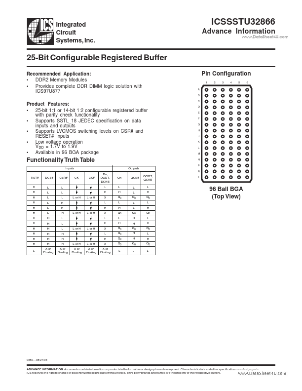
Datasheet4U Logo Datasheet4U.com

ICSSSTU32866 - 25-Bit Configurable Registered Buffer

General Description

This 25-bit 1:1 or 14-bit 1:2 configurable registered buffer is designed for 1.7-V to 1.9-V VDD operation.

All clock and data inputs are compatible with the JEDEC standard for SSTL_18.

The control inputs are LVCMOS.

Key Features

  • 25-bit 1:1 or 14-bit 1:2 configurable registered buffer with parity check functionality.
  • Supports SSTL_18 JEDEC specification on data inputs and outputs.
  • Supports LVCMOS switching levels on CSR# and RESET# inputs.
  • Low voltage operation VDD = 1.7V to 1.9V.
  • Available in 96 BGA package Pin Configuration 1 A B C D E F G H J K L M N P 2 3 4 5 6 Functionality Truth Table I nputs RST# H H H H H H H H H H H H L DCS# L L L L L L H H H H H H X or Floating C.

📥 Download Datasheet

Datasheet Details

Part number ICSSSTU32866
Manufacturer Integrated Circuit System
File Size 202.68 KB
Description 25-Bit Configurable Registered Buffer
Datasheet download datasheet ICSSSTU32866 Datasheet

Full PDF Text Transcription for ICSSSTU32866 (Reference)

Note: Below is a high-fidelity text extraction (approx. 800 characters) for ICSSSTU32866. For precise diagrams, and layout, please refer to the original PDF.

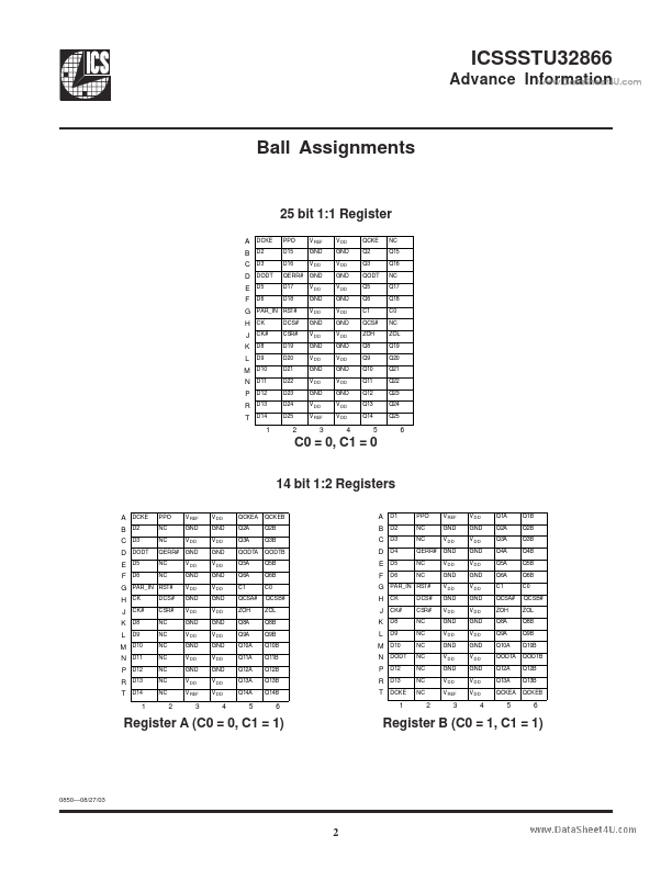
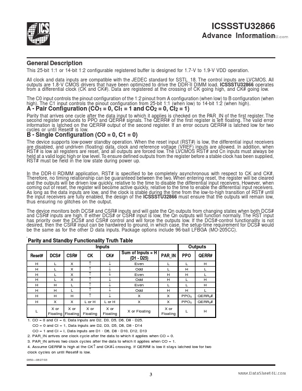
Integrated Circuit Systems, Inc. ICSSSTU32866 Advance Information www.DataSheet4U.com 25-Bit Configurable Registered Buffer Recommended Application: • DDR2 Memory Modules...

View more extracted text
rable Registered Buffer Recommended Application: • DDR2 Memory Modules • Provides complete DDR DIMM logic solution with ICS97U877 Product Features: • 25-bit 1:1 or 14-bit 1:2 configurable registered buffer with parity check functionality • Supports SSTL_18 JEDEC specification on data inputs and outputs • Supports LVCMOS switching levels on CSR# and RESET# inputs • Low voltage operation VDD = 1.7V to 1.