Datasheet Summary
..
ICS570A Multiplier and Zero Delay Buffer
Description
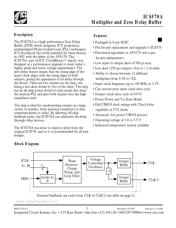
The ICS570A is a high performance Zero Delay Buffer (ZDB) which integrates ICS’ proprietary analog/digital Phase Locked Loop (PLL) techniques. ICS introduced the world standard for these devices in 1992 with the debut of the AV9170. The ICS570A, part of ICS’ ClockBlocks™ family, was designed as a performance upgrade to meet today’s higher speed and lower voltage requirements. The zero delay feature means that the rising edge of the input clock aligns with the rising edges of both outputs, giving the appearance of no delay through the device. There are two outputs on the chip, one being a low-skew divide by two of the...