ICS570 Overview
Description
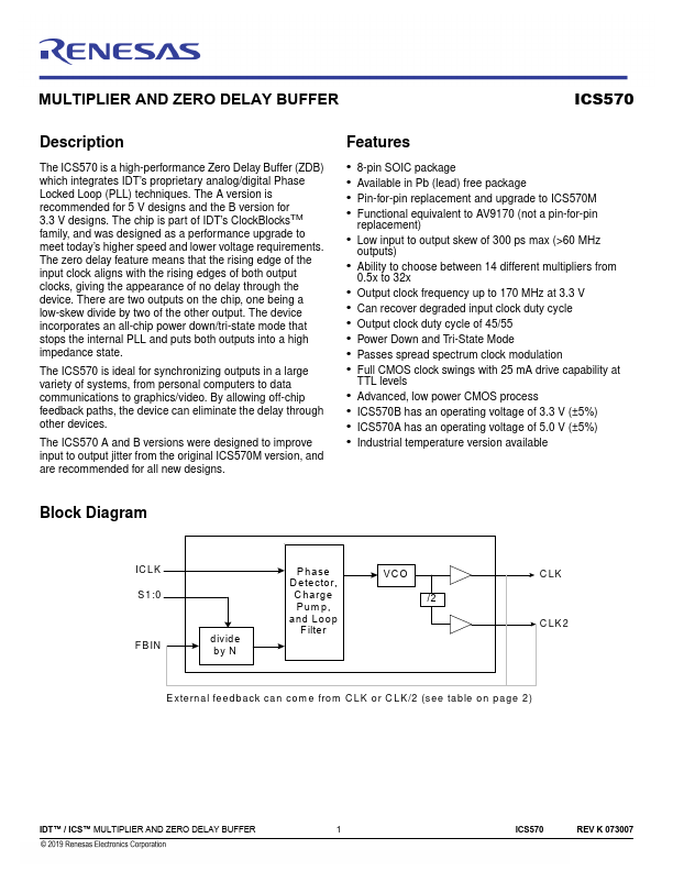
The ICS570 is a high-performance Zero Delay Buffer (ZDB) which integrates IDT’s proprietary analog/digital Phase Locked Loop (PLL) techniques. The A version is recommended for 5 V designs and the B version for 3.3 V designs.
Key Features
- 8-pin SOIC package
- Available in Pb (lead) free package
- Pin-for-pin replacement and upgrade to ICS570M
- Functional equivalent to AV9170 (not a pin-for-pin replacement)
- Low input to output skew of 300 ps max (>60 MHz outputs)
- Ability to choose between 14 different multipliers from 0.5x to 32x
- Output clock frequency up to 170 MHz at 3.3 V
- Can recover degraded input clock duty cycle
- Output clock duty cycle of 45/55
- Power Down and Tri-State Mode