ICS952606
ICS952606 is Programmable Timing Control Hub for Next Gen P4 processor manufactured by Integrated Circuit Systems.
Integrated Circuit Systems, Inc.
Programmable Timing Control Hub™ for Next Gen P4™ processor
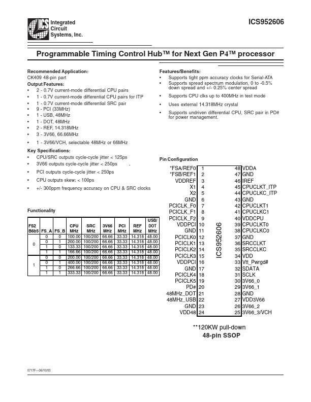
Remended Application: CK409 48-pin part Output Features
:
- 2
- 0.7V current-mode differential CPU pairs
- 1
- 0.7V current-mode differential CPU pairs for ITP
- 1
- 0.7V current-mode differential SRC pair
- 9
- PCI (33MHz)
- 1
- USB, 48MHz
- 1
- DOT, 48MHz
- 2
- REF, 14.318MHz
- 3
- 3V66, 66.66MHz
- 1
- 3V66/VCH, selectable 48MHz or 66MHz Features
/Benefits:
- Supports tight ppm accuracy clocks for Serial-ATA
- Supports spread spectrum modulation, 0 to -0.5% down spread and +/- 0.25% center spread
- -
- Supports CPU clks up to 400MHz in test mode Uses external 14.318MHz crystal...