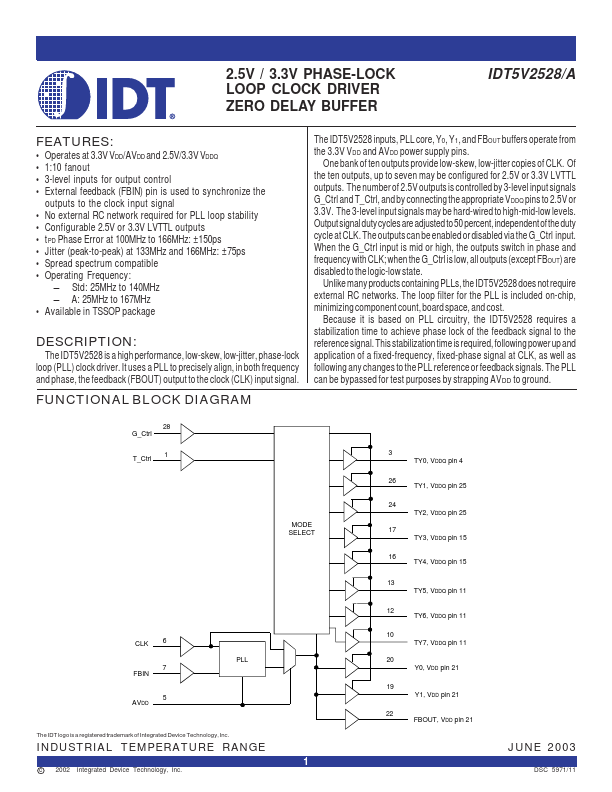
IDT5V2528 Overview
The IDT5V2528 is a high performance, low-skew, low-jitter, phase-lock loop (PLL) clock driver. It uses a PLL to precisely align, in both frequency and phase, the feedback (FBOUT) output to the clock (CLK) input signal. FUNCTIONAL BLOCK DIAGRAM The IDT5V2528 inputs, PLL core, Y0, Y1, and FBOUT buffers operate from the 3.3V VDD and AVDD power supply pins.
IDT5V2528 Key Features
- Operates at 3.3V VDD/AVDD and 2.5V/3.3V VDDQ
- 1:10 fanout
- 3-level inputs for output control
- External feedback (FBIN) pin is used to synchronize the
- No external RC network required for PLL loop stability
- Configurable 2.5V or 3.3V LVTTL outputs
- tPD Phase Error at 100MHz to 166MHz: ±150ps
- Jitter (peak-to-peak) at 133MHz and 166MHz: ±75ps
- Spread spectrum patible
- Operating Frequency