8V44N4614 Overview
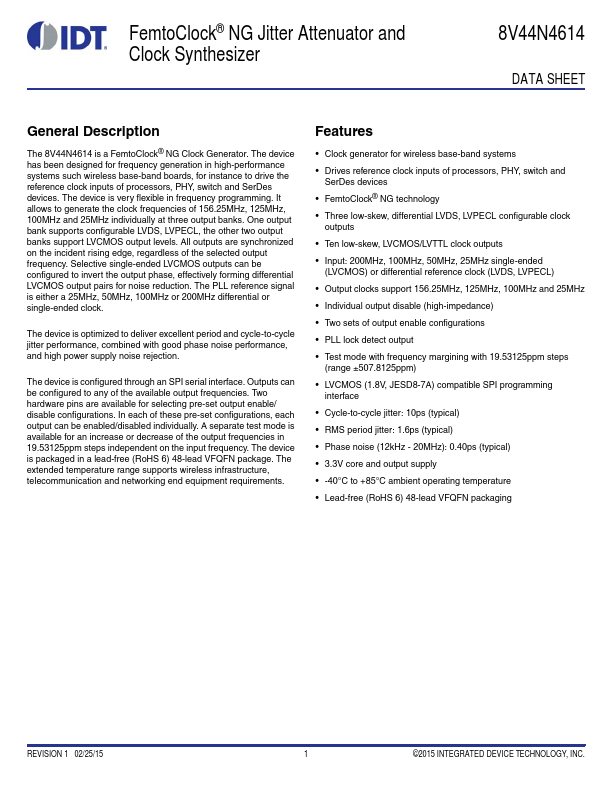
The 8V44N4614 is a FemtoClock® NG Clock Generator. The device has been designed for frequency generation in high-performance systems such wireless base-band boards, for instance to drive the reference clock inputs of processors, PHY, switch and SerDes devices. The device is very flexible in frequency programming.
8V44N4614 Key Features
- Clock generator for wireless base-band systems
- Drives reference clock inputs of processors, PHY, switch and
- FemtoClock® NG technology
- Three low-skew, differential LVDS, LVPECL configurable clock
- Ten low-skew, LVCMOS/LVTTL clock outputs
- Input: 200MHz, 100MHz, 50MHz, 25MHz single-ended
- Output clocks support 156.25MHz, 125MHz, 100MHz and 25MHz
- Individual output disable (high-impedance)
- Two sets of output enable configurations
- PLL lock detect output