ICS831724I Overview
Description
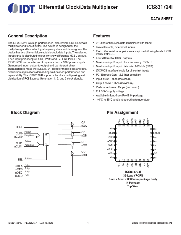
The ICS831724I is a high-performance, differential HCSL clock/data multiplexer and fanout buffer. The device is designed for the multiplexing and fanout of high-frequency clock and data signals.
Key Features
- 2:1 differential clock/data multiplexer with fanout
- Two selectable, differential inputs
- Each differential input pair can accept the following levels: HCSL, LVDS, LVPECL
- Four differential HCSL outputs
- Maximum input/output clock frequency: 350MHz