IDT72T72105
Overview
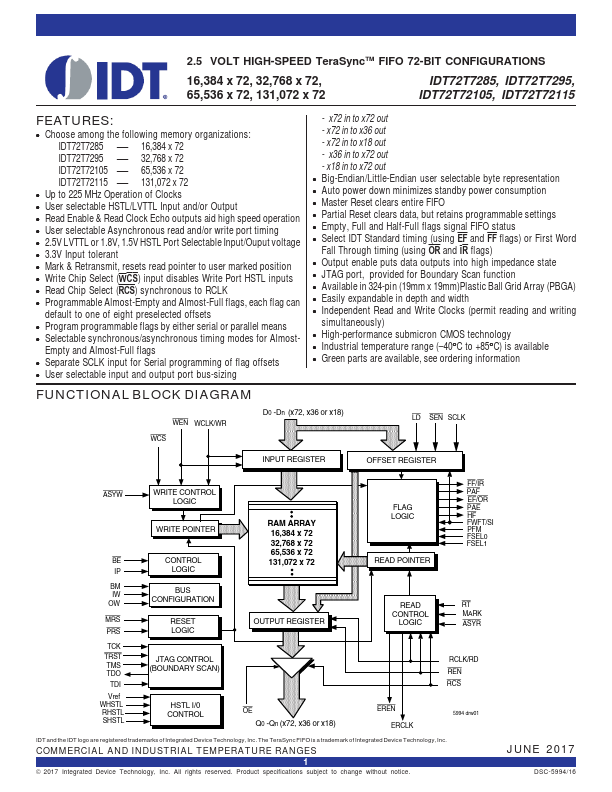
- Choose among the following memory organizations: IDT72T7285 16,384 x 72 IDT72T7295 32,768 x 72 IDT72T72105 65,536 x 72 IDT72T72115 131,072 x 72 Up to 225 MHz Operation of Clocks User selectable HSTL/LVTTL Input and/or Output Read Enable & Read Clock Echo outputs aid high speed operation User selectable Asynchronous read and/or write port timing 2.5V LVTTL or 1.8V, 1.5V HSTL Port Selectable Input/Ouput voltage 3.3V Input tolerant Mark & Retransmit, resets read pointer to user marked position Write Chip Select (WCS) input disables Write Port HSTL inputs Read Chip Select (RCS) synchronous to RCLK Programmable Almost-Empty and Almost-Full flags, each flag can default to one of eight preselected offsets Program programmable flags by either serial or parallel means Selectable synchronous/asynchronous timing modes for AlmostEmpty and Almost-Full flags Separate SCLK input for Serial programming of flag offsets * * * * * * * * * * * *
- User selectable input and output port bus-sizing - x72 in to x72 out - x72 in to x36 out - x72 in to x18 out - x36 in to x72 out - x18 in to x72 out Big-Endian/Little-Endian user selectable byte representation Auto power down minimizes standby power consumption Master Reset clears entire FIFO Partial Reset clears data, but retains programmable settings Empty, Full and Half-Full flags signal FIFO status Select IDT Standard timing (using EF and FF flags) or First Word Fall Through timing (using OR and IR flags) Output enable puts data outputs into high impedance state JTAG port, provided for Boundary Scan function Available in 324-pin (19mm x 19mm)Plastic Ball Grid Array (PBGA) Easily expandable in depth and width Independent Read and Write Clocks (p