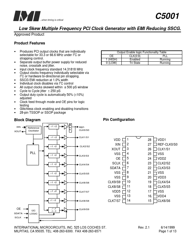
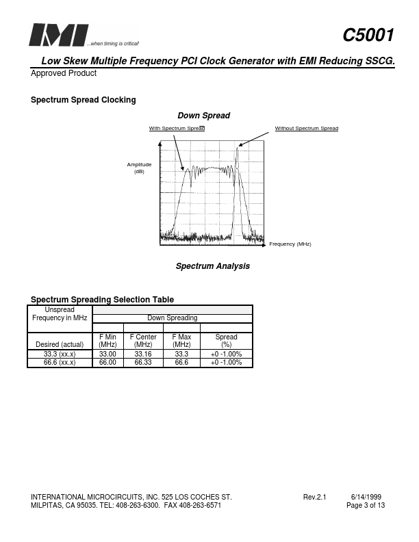
Datasheet4U Logo Datasheet4U.com

C5001 - Low Skew Muliple Frequency PCI Clock Generator with EMI Reducing SSCG

Description

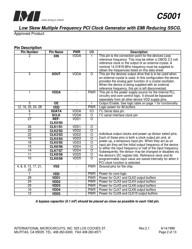
Pin Number 2 Pin Name XIN PWR VDDA I/O I Description This pin is the connection point for the devices Loop reference frequency.

This may be either a CMOS 3.3 volt reference clock or the output of an external crystal.

Features

  • S S S S S S S S S S S S Produces PCI output clocks that are individually 2 selectable for 33.3 or 66.6 MHz under I C or strapping control. Separate output buffer power supply for reduced noise, crosstalk and jitter. input clock frequency standard 14.31818 MHz Output clocks frequency individually selectable via 2 I C or hardware bi-directional pin strapping. SSCG EMI reduction at 1.0% width 2 Individual clock disables via I C control All output clocks skewed within a 500 pS window Cycle to Cycle.

📥 Download Datasheet

Datasheet Details

Part number C5001
Manufacturer International
File Size 138.21 KB
Description Low Skew Muliple Frequency PCI Clock Generator with EMI Reducing SSCG
Datasheet download datasheet C5001 Datasheet
Other Datasheets by International

Full PDF Text Transcription

Click to expand full text
C5001 Low Skew Multiple Frequency PCI Clock Generator with EMI Reducing SSCG. Approved Product Product Features S S S S S S S S S S S S Produces PCI output clocks that are individually 2 selectable for 33.3 or 66.6 MHz under I C or strapping control. Separate output buffer power supply for reduced noise, crosstalk and jitter. input clock frequency standard 14.31818 MHz Output clocks frequency individually selectable via 2 I C or hardware bi-directional pin strapping. SSCG EMI reduction at 1.
Published: |