C5002
Key Features
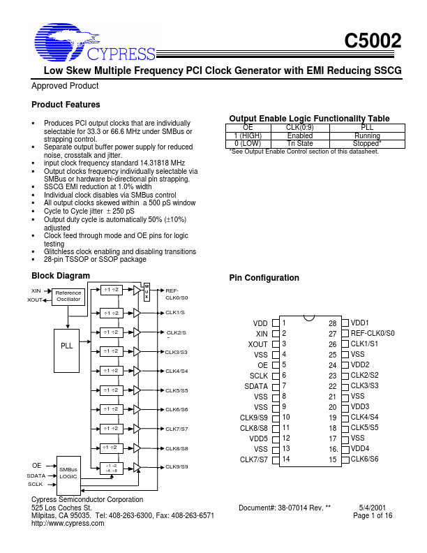
- See Output Enable Control section of this datasheet.
| Part Number | Manufacturer | Description |
|---|---|---|
| C5002 | Sanken | 2SC5002 |
| C5002 | SavantIC | 2SC5002 |
| LEF-C5002T | Letex | FULL COLOR LED LAMPS |
| LEF-C5001T | Unknown Manufacturer | FULL COLOR LED LAMPS |