IRF7752 Overview
Key Specifications
Package: TSSOP
Mount Type: Surface Mount
Pins: 8
Height: 1.0414 mm
Description
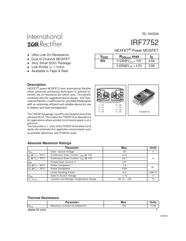
HEXFET® power MOSFETs from International Rectifier utilize advanced processing techniques to achieve extremely low on-resistance per silicon area. This benefit, combined with the ruggedized device design , that International Rectifier is well known for, provides thedesigner 1 2 3 4 1= 2= 3= 4= D1 S1 S1 G1 8= 7= 6= 5= 8 7 6 5 D2 S2 S2 G2 with an extremely efficient and reliable device for use in battery and load management.