IRFB3607GPBF Description
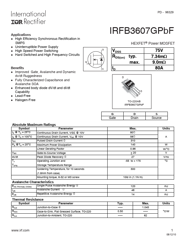
PD - 96329 Applications l High Efficiency Synchronous Rectification in SMPS l Uninterruptible Power Supply l High Speed Power Switching l Hard Switched and High Frequency Circuits G IRFB3607GPbF HEXFET® Power MOSFET D Benefits l Improved Gate, Avalanche and Dynamic dv/dt Ruggedness l Fully Characterized Capacitance and Avalanche SOA l Enhanced body diode dV/dt and dI/dt Capability l Lead-Free l Halogen-Free S VDSS...
IRFB3607GPBF Key Features
- High Efficiency Synchronous Rectification in SMPS
- Uninterruptible Power Supply
- High Speed Power Switching
- Hard Switched and High Frequency Circuits G IRFB3607GPbF HEXFET® Power MOSFET D Benefits
- Improved Gate, Avalanche and Dynamic dv/dt Ruggedness
- Fully Characterized Capacitance and Avalanche SOA
- Enhanced body diode dV/dt and dI/dt Capability
- Lead-Free