IRFHM4234TRPBF Overview
Key Specifications
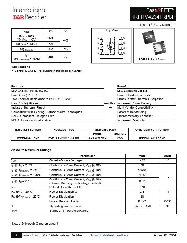
Mount Type: Surface Mount
Height: 900 µm
Length: 3.3 mm
Width: 3.3 mm
| Part | IRFHM4234TRPBF |
|---|---|
| Description | Power MOSFET |
| Category | MOSFET |
| Manufacturer | International Rectifier |
| Size | 568.53 KB |
Mount Type: Surface Mount
Height: 900 µm
Length: 3.3 mm
Width: 3.3 mm
| Seller | Inventory | Price Breaks | Buy |
|---|---|---|---|
| Rochester Electronics | 1122 | 100+ : 0.4573 USD 500+ : 0.4116 USD 1000+ : 0.3796 USD 10000+ : 0.3384 USD |
View Offer |
| Avnet | 0 | 1+ : 1.3 USD 10+ : 1.19 USD 25+ : 1.11 USD 50+ : 1.03 USD |
View Offer |
| Part Number | Manufacturer | Description |
|---|---|---|
| AP9563GH | Advanced Power Electronics Corp | P-CHANNEL ENHANCEMENT MODE POWER MOSFET |
| A2SHB | HAOHAI | N-Channel MOSFET |
| FCPF360N65S3R0L | onsemi | N-Channel MOSFET |