IRFP2907B
IRFP2907B is HEXFET Power MOSFET manufactured by International Rectifier.
..
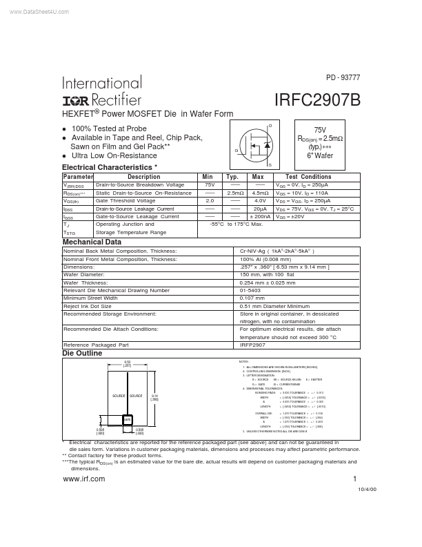
- 93777
IRFC2907B
HEXFET® l
Power MOSFET Die in Wafer Form
100% Tested at Probe l Available in Tape and Reel, Chip Pack, Sawn on Film and Gel Pack-
- l Ultra Low On-Resistance Electrical Characteristics
- Parameter V(BR)DSS RDS(on)-
- - VGS(th) IDSS IGSS TJ TSTG Description Drain-to-Source Breakdown Voltage Static Drain-to-Source On-Resistance Gate Threshold Voltage Drain-to-Source Leakage Current Gate-to-Source Leakage Current Operating Junction and Storage Temperature Range
75V RDS(on) = 2.5mΩ (typ.)∗∗∗ 6" Wafer
Test Conditions VGS = 0V, ID = 250µA VGS = 10V, ID = 110A V DS = VGS, ID = 250µA VDS = 75V, VGS = 0V, TJ = 25°C V GS = ±20V
Min Typ. Max 75V
- -
- -
-...