ISL75051SRH Description
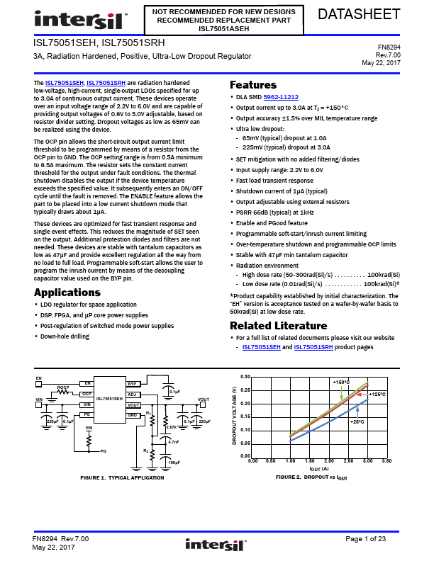
These devices operate over an input voltage range of 2.2V to 6.0V and are capable of providing output voltages of 0.8V to 5.0V adjustable, based on resistor divider setting. Dropout voltages as low as 65mV can be realized using the device. The OCP pin allows the short-circuit output current limit threshold to be programmed by means of a resistor from the OCP pin to GND.
ISL75051SRH Key Features
- DLA SMD 5962-11212
- Output current up to 3.0A at TJ = +150°C
- Output accuracy ±1.5% over MIL temperature range
- Ultra low dropout
- 65mV (typical) dropout at 1.0A
- 225mV (typical) dropout at 3.0A
- SET mitigation with no added filtering/diodes
- Input supply range: 2.2V to 6.0V
- Fast load transient response
- Shutdown current of 1µA (typical)
ISL75051SRH Applications
- LDO regulator for space application