CD4015BMS
Overview
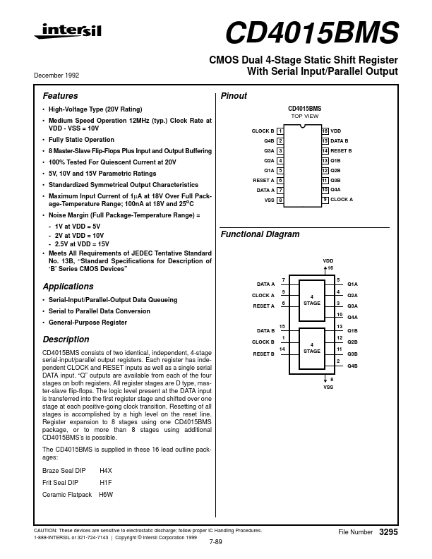
CD4015BMS consists of two identical, independent, 4-stage serial-input/parallel output registers. Each register has independent CLOCK and RESET inputs as well as a single serial DATA input. “Q” outputs are available from each of the four stages on both registers.
- High-Voltage Type (20V Rating)
- Medium Speed Operation 12MHz (typ.) Clock Rate at VDD - VSS = 10V
- Fully Static Operation
- 8 Master-Slave Flip-Flops Plus Input and Output Buffering
- 100% Tested For Quiescent Current at 20V
- 5V, 10V and 15V Parametric Ratings
- Standardized Symmetrical Output Characteristics
- Maximum Input Current of 1µA at 18V Over Full Package-Temperature Range; 100nA at 18V and 25oC
- Noise Margin (Full Package-Temperature Range) = - 1V at VDD = 5V - 2V at VDD = 10V - 2.5V at VDD = 15V
- Meets All Requirements of JEDEC Tentative Standard No. 13B, “Standard Specifications for Description of ‘B’ Series CMOS Devices”