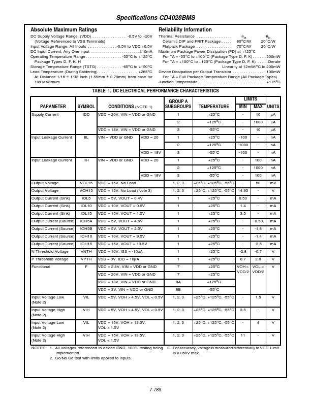
Datasheet Summary
December 1992
CMOS BCD-To-Decimal Decoder
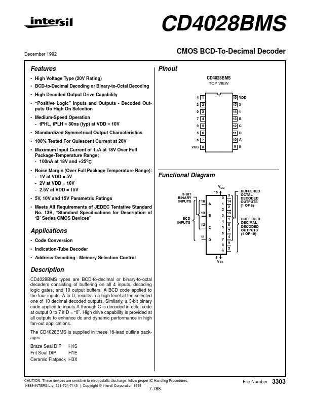
Pinout
CD4028BMS TOP VIEW
Features
- High Voltage Type (20V Rating)
- BCD-to-Decimal Decoding or Binary-to-Octal Decoding
- High Decoded Output Drive Capability
- “Positive Logic” Inputs and Outputs
- Decoded Outputs Go High On Selection
- Medium-Speed Operation
- tPHL, tPLH = 80ns (typ) at VDD = 10V
- Standardized Symmetrical Output Characteristics
- 100% Tested For Quiescent Current at 20V
- Maximum Input Current of 1µA at 18V Over Full Package-Temperature Range;
- 100nA at 18V and +25oC
- Noise Margin (Over Full Package Temperature Range):
- 1V at VDD = 5V
- 2V at VDD = 10V
- 2.5V at VDD = 15V
- 5V, 10V and 15V Parametric Ratings
-...