CD4041UBMS
Features
- High Voltage Type (20V Rating)
- Balanced Sink and Source Current; Approximately 4 Times Standard “B” Drive
- Equalized Delay to True and plement Outputs
- 100% Tested for Quiescent Current at 20V
- Maximum Input Current of 1µA at 18V Over Full Package-Temperature Range;
- 100n A at 18V and +25o C
- 5V, 10V and 15V Parametric Ratings
- Meets All Requirements of JEDEC Tentative Standard No. 13B, “Standard Specificationsfor Description of ‘B’ Series CMOS Devices”
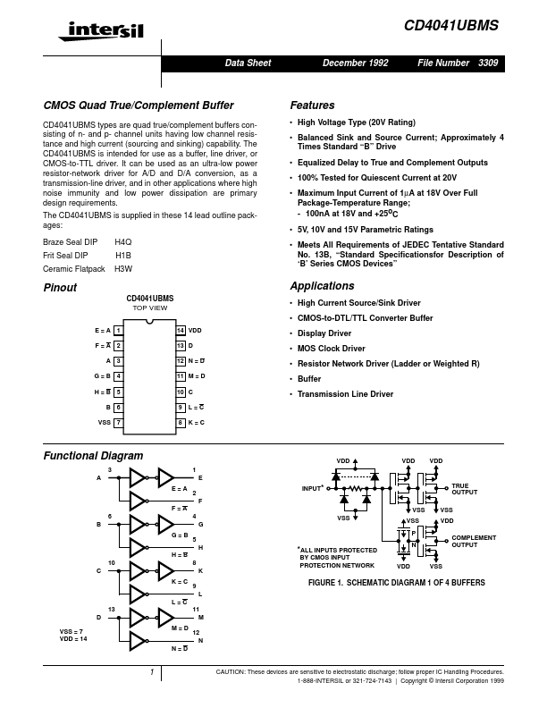
Pinout
CD4041UBMS TOP VIEW
E=A 1 F=A 2 A 3 G=B 4 H=B 5 B 6 VSS 7 14 VDD 13 D 12 N = D 11 M = D 10 C 9 L=C 8 K=C
Applications
- High Current Source/Sink Driver
- CMOS-to-DTL/TTL Converter Buffer
- Display Driver
- MOS Clock Driver
- Resistor Network Driver (Ladder or Weighted R)
- Buffer
- Transmission Line Driver
Functional Diagram
3 A E=A F=A 6 B G=B H=B 10 C K=C L=C 13 D VSS = 7 VDD = 14 M=D N=D 11 M 12 N 9 L 8 K 5 H 4 G 2 F 1 E INPUT-
TRUE OUTPUT VSS VSS VSS P VSS VDD PLEMENT OUTPUT
- ALL INPUTS...