Datasheet4U Logo Datasheet4U.com

CD4042BMS - CMOS Quad Clocked D-Latch

General Description

of ‘B’ Series CMOS Devices” Q4 1 Q1 2 Q1 3 D1 4 CLOCK 5 POLARITY 6 D2 7 VSS 8 NC = NO CONNECTION 16 VDD 15 Q4 14 D4 13 D3 12 Q3 11 Q3 10 Q2 9 Q2 Functional Diagram D1 4 2 3 D2 7 10 9 D3 13 11 12 D4 14 1 15 CLOCK 5 CL Q1 Q1 Q2 Q2 Q3 Q3 Q4 Q4 Applications • Buffer Storage • Holding Register • General Digital Logic Description 
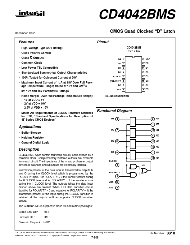
CD4042BMS types contain four latch circuits, each strobed by a common clock.

Complementary buffered outputs are available from each circuit.

The impedance of the n- and p- channel output devices is balanced and all outputs are electrically identical.

Overview

CD4042BMS December 1992 CMOS Quad Clocked “D” Latch Pinout CD4042BMS TOP.

Key Features

  • High-Voltage Type (20V Rating).
  • Clock Polarity Control.
  • Q and Q Outputs.
  • Common Clock.
  • Low Power TTL Compatible.
  • Standardized Symmetrical Output Characteristics.
  • 100% Tested for Quiescent Current at 20V.
  • Maximum Input Current of 1µA at 18V Over Full Package Temperature Range; 100nA at 18V and +25oC.
  • 5V, 10V and 15V Parametric Ratings.
  • Noise Margin (Over Full Package Temperature Range): - 1V at VDD = 5V - 2.