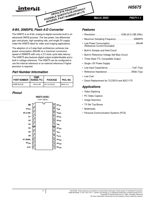
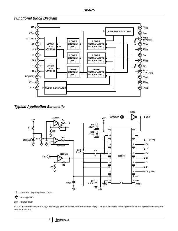
HI5675 converter equivalent, flash a/d converter.
digital output enable/disable and a built in voltage reference. The HI5675 can be configured to use the internal reference or an external reference if higher precision is.
The adoption of a 2-step flash architecture achieves low power consumption (60mW) at a maximum conversion speed of 20MS.
PIN NUMBER 1 2, 24 3-10 11, 13 12 16 17 23 14, 15, 18 19 20, 21 22 SYMBOL OE DVSS D0 to D7 DVDD CLK VRTS VRT VRB AVDD VIN AVSS VRBS DESCRIPTION When OE = Low, Data is valid. When OE = High, D0 to D7 pins high impedance. Digital GND. D0 (LSB) to D7 (.
Image gallery
TAGS