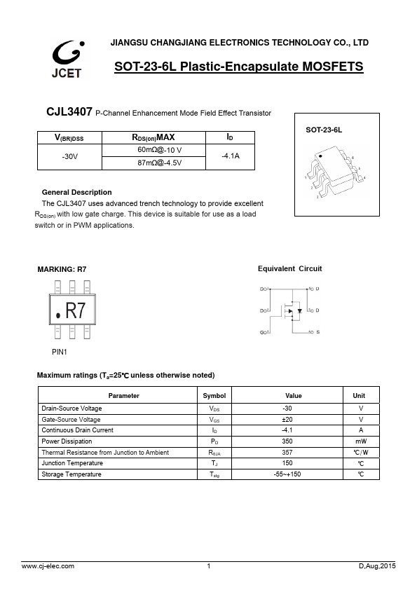
Datasheet4U Logo Datasheet4U.com

CJL3407 Datasheet P-Channel MOSFET

Manufacturer: JCET

Datasheet Details

Part number CJL3407
Manufacturer JCET
File Size 760.14 KB
Description P-Channel MOSFET
Download CJL3407 Download (PDF)

General Description

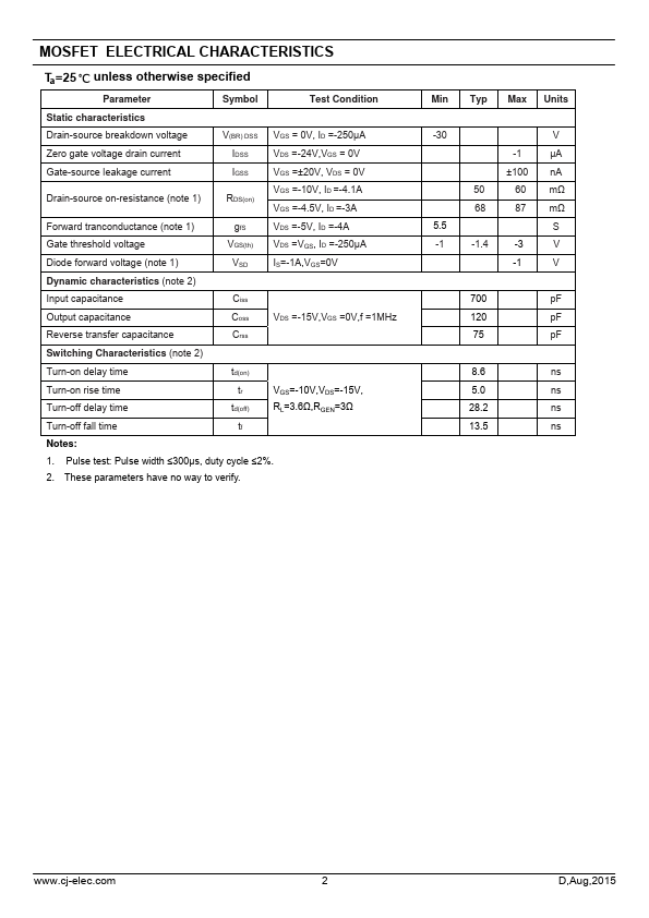
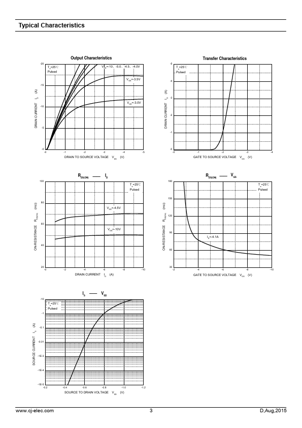
The CJL3407 uses advanced trench technology to provide excellent RDS(on) with low gate charge.

This device is suitable for use as a load switch or in PWM applications.

SOT-23-6L MARKING: R7 Equivalent Circuit PIN1 Maximum ratings (Ta=25℃ unless otherwise noted) Parameter Drain-Source Voltage Gate-Source Voltage Continuous Drain Current Power Dissipation Thermal Resistance from Junction to Ambient Junction Temperature Storage Temperature Symbol VDS VGS ID PD RθJA TJ Tstg Value -30 ±20 -4.1 350 357 150 -55~+150 Unit V V A mW ℃/W ℃ ℃ www.cj-elec.com 1 D,Aug,2015 MOSFET ELECTRICAL CHARACTERISTICS Ta=25 ℃ unless otherwise specified Parameter Symbol Test Condition Static characteristics Drain-source breakdown voltage V(BR) DSS VGS = 0V, ID =-250µA Zero gate voltage drain current IDSS VDS =-24V,VGS = 0V Gate-source leakage current IGSS VGS =±20V, VDS = 0V Drain-source on-resistance (note 1) RDS(on) VGS =-10V, ID =-4.1A VGS =-4.5V, ID =-3A Forward tranconductance (note 1) gfS VDS =-5V, ID =-4A Gate threshold voltage VGS(th) VDS =VGS, ID =-250µA Diode forward voltage (note 1) VSD IS=-1A,VGS=0V Dynamic characteristics (note 2) Input capacitance Ciss Output capacitance Coss VDS =-15V,VGS =0V,f =1MHz Reverse transfer capacitance Crss Switching Characteristics (note 2) Turn-on delay time td(on) Turn-on rise time Turn-off delay time tr td(off) VGS=-10V,VDS=-15V, RL=3.6Ω,RGEN=3Ω Turn-off fall time tf Notes: 1.

Overview

JIANGSU CHANGJIANG ELECTRONICS TECHNOLOGY CO., LTD SOT-23-6L Plastic-Encapsulate MOSFETS CJL3407 P-Channel Enhancement Mode Field Effect Transistor V(BR)DSS -30V RDS(on)MAX 60mΩ@-10 V 87mΩ@-4.5V ID -4.