Click to expand full text
PT4435
30V P-Channel Enhancement Mode MOSFET
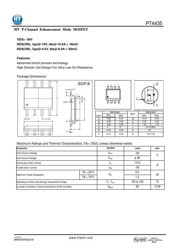
VDS= -30V RDS(ON), Vgs@-10V, Ids@-10.5A = 18mΩ RDS(ON), Vgs@-4.5V, Ids@-6.0A = 30mΩ Features Advanced trench process technology High Density Cell Design For Ultra Low On-Resistance Package Dimensions
D 8 D 7 D 6 D 5
1 S S
2 S
3
4 G
http://www.DataSheet4U.net/
REF. A B C D E F
Millimeter Min. Max.
5.80 4.80 3.80 0° 0.40 0.19 6.20 5.00 4.00 8° 0.90 0.25
REF. M H L J K G
Millimeter Min. Max.
0.10 0.25 0.35 0.49 1.35 1.75 0.375 REF. 45° 1.27 TYP.
Maximum Ratings and Thermal Characteristics (TA = 25oC unless otherwise noted)
Parameter Drain-Source Voltage Gate-Source Voltage Continuous Drain Current Pulsed Drain Current Symbol Limit Unit
VDS VGS ID IDM TA = 25 C
o o
-30 ± 20 -10.5 -50 2.5 1.
 PT4435 Datasheet