High Voltage : BVDSS=650V(Min. ) Low Crss : Crss=5.6pF(Typ. ) Low gate charge : Qg=11.2nC(Typ. ) Low RDS(on) : RDS(on)=3.0Ω(Max. )
G Package Code TO-252 S TO-252 S Type No. SMK0465D Marking SMK0465
PIN Connection
D D
G
Ordering Information
Marking Diagram
Column 1 2 : Device Code Column 3: Production Information e. g. ) YWW -. Y: Year Code -. WW: Week Code
Absolute maximum ratings (TC=25C unless otherwise noted)
Characteristic
Drain-source voltage Gate-source voltage Drai.
The following content is an automatically extracted verbatim text
from the original manufacturer datasheet and is provided for reference purposes only.
View original datasheet text
SMK0465D
Advanced Power N-Ch MOSFET
SWITCHING REGULATOR APPLICATIONS Features
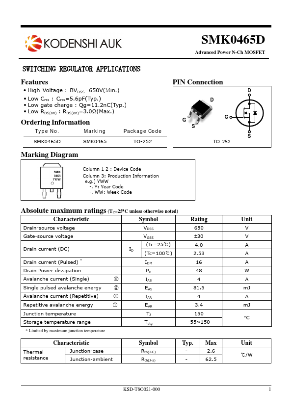
High Voltage : BVDSS=650V(Min.) Low Crss : Crss=5.6pF(Typ.) Low gate charge : Qg=11.2nC(Typ.) Low RDS(on) : RDS(on)=3.0Ω(Max.)
G Package Code TO-252 S TO-252 S Type No. SMK0465D Marking SMK0465
PIN Connection
D D
G
Ordering Information
Marking Diagram
Column 1 2 : Device Code Column 3: Production Information e.g.) YWW -. Y: Year Code -. WW: Week Code
Absolute maximum ratings (TC=25C unless otherwise noted)
Characteristic
Drain-source voltage Gate-source voltage Drain current (DC) Drain current (Pulsed)
*
Symbol
VDSS VGSS ID (Tc=25℃) (Tc=100℃) IDM PD ② ② ① ① IAS EAS IAR EAR TJ Tstg
Rating
650 30 4.0 2.53 16 48 4 81.5 4 3.