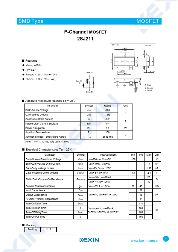
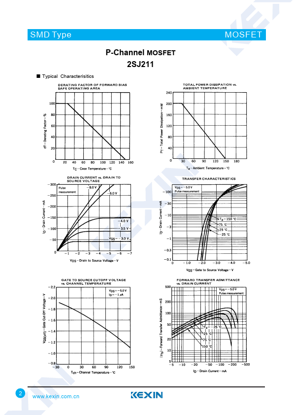
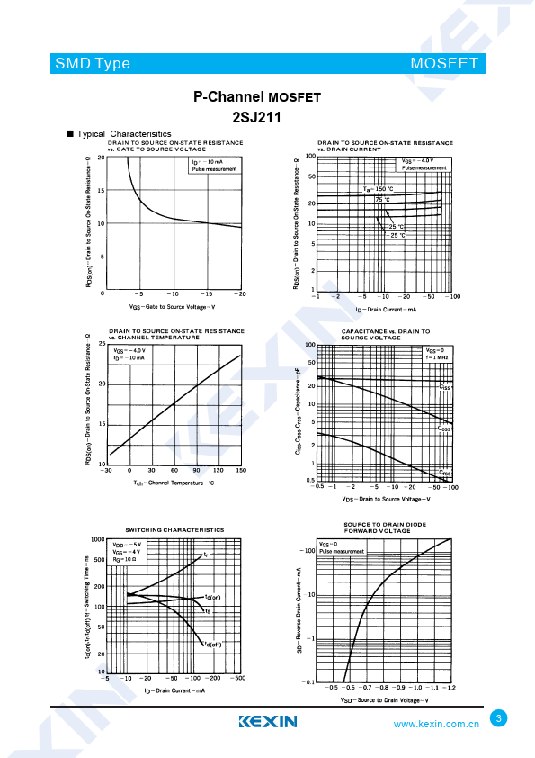
Datasheet4U Logo Datasheet4U.com

2SJ211 - P-Channel MOSFET

Key Features

  • s.
  • VDS (V) =-100V.
  • ID =-0.2 A.
  • RDS(ON) < 20Ω (VGS =-10V).
  • RDS(ON) < 30Ω (VGS =-4V) P-Channel MOSFET 2SJ211 SOT-23 2.9 +0.1 -0.1 0.4 +0.1 -0.1 3 +0.12.4 -0.1 12 0.95 +0.1 -0.1 1.9 +0.1 -0.1 +0.10.97 -0.1 +0.11.3 -0.1 0.55 0.4 MOSFET Unit: mm 0.1 +0.05 -0.01 1. Gate 2. Source 3. Drain 0-0.1 +0.10.38 -0.1.
  • Absolute Maximum Ratings Ta = 25℃ Parameter Drain-Source Voltage Gate-Source Voltage Continuous Drain Current Pulsed Drain Current (Note.1) Power Dissipation Ju.

📥 Download Datasheet

Full PDF Text Transcription for 2SJ211 (Reference)

Note: Below is a high-fidelity text extraction (approx. 800 characters) for 2SJ211. For precise diagrams, and layout, please refer to the original PDF.

SMD Type ■ Features ● VDS (V) =-100V ● ID =-0.2 A ● RDS(ON) < 20Ω (VGS =-10V) ● RDS(ON) < 30Ω (VGS =-4V) P-Channel MOSFET 2SJ211 SOT-23 2.9 +0.1 -0.1 0.4 +0.1 -0.1 3 +0.1...

View more extracted text
-4V) P-Channel MOSFET 2SJ211 SOT-23 2.9 +0.1 -0.1 0.4 +0.1 -0.1 3 +0.12.4 -0.1 12 0.95 +0.1 -0.1 1.9 +0.1 -0.1 +0.10.97 -0.1 +0.11.3 -0.1 0.55 0.4 MOSFET Unit: mm 0.1 +0.05 -0.01 1. Gate 2. Source 3. Drain 0-0.1 +0.10.38 -0.1 ■ Absolute Maximum Ratings Ta = 25℃ Parameter Drain-Source Voltage Gate-Source Voltage Continuous Drain Current Pulsed Drain Current (Note.1) Power Dissipation Junction Temperature Junction Storage Temperature Range Note.1: PW ≤ 10 ms, duty cycle ≤ 50% Symbol VDS VGS ID IDM PD TJ Tstg Rating -100 ±20 -0.2 -0.4 0.