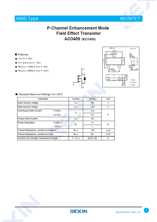
Datasheet4U Logo Datasheet4U.com

KO3409 - P-Channel MOSFET

Key Features

  • VDS (V) = -30V ID = -2.6 A (VGS = -10V) RDS(ON) < 130m (VGS = -10V) RDS(ON) < 200m (VGS = -4.5V) +0.12.4 -0.1 SOT-23 2.9 +0.1 -0.1 0.4 +0.1 -0.1 3 12 0.95 +0.1 -0.1 1.9 +0.1 -0.1 +0.11.3 -0.1 0.55 0.4 Unit: mm 0.1 +0.05 -0.01 +0.10.97 -0.1 0-0.1 +0.10.38 -0.1 11.. BGasaete 22.. ESmiotutrecre 33.. cDolrlaeicntor Absolute Maximum Ratings Ta = 25 Parameter Drain-Source Voltage Gate-Source Voltage Continuous Drain Current TA=25 TA=70 Pulsed Drain Current Power Dissipation TA=25 TA=70.

📥 Download Datasheet

Full PDF Text Transcription (Reference)

The following content is an automatically extracted verbatim text from the original manufacturer datasheet and is provided for reference purposes only.

View original datasheet text
SMD Type P-Channel Enhancement Mode Field Effect Transistor AO3409 (KO3409) MOSFET Features VDS (V) = -30V ID = -2.6 A (VGS = -10V) RDS(ON) < 130m (VGS = -10V) RDS(ON) < 200m (VGS = -4.5V) +0.12.4 -0.1 SOT-23 2.9 +0.1 -0.1 0.4 +0.1 -0.1 3 12 0.95 +0.1 -0.1 1.9 +0.1 -0.1 +0.11.3 -0.1 0.55 0.4 Unit: mm 0.1 +0.05 -0.01 +0.10.97 -0.1 0-0.1 +0.10.38 -0.1 11.. BGasaete 22..ESmiotutrecre 33..cDolrlaeicntor Absolute Maximum Ratings Ta = 25 Parameter Drain-Source Voltage Gate-Source Voltage Continuous Drain Current TA=25 TA=70 Pulsed Drain Current Power Dissipation TA=25 TA=70 Themal Resistance. Junction-to-Ambient Themal Resistance. Junction-to-Case Junction and Storage Temperature Range Symbol VDS VGS ID IDM PD RthJA RthJC TJ, TSTG Rating -30 20 -2.6 -2.2 -20 1.