ML145408 Overview
Key Features
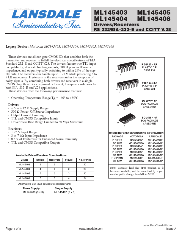
- Operating Temperature Range TA = –40° to +85°C Drivers
- ± 5 to ± 12 V Supply Range
- 300 Ω Power–Off Source Impedance
- Output Current Limiting
- TTL and CMOS Compatible Inputs
| Part | ML145408 |
|---|---|
| Description | Drivers/Receivers |
| Manufacturer | LANSDALE Semiconductor |
| Size | 521.46 KB |
| Part Number | Manufacturer | Description |
|---|---|---|
| MAX232 | Maxim Integrated | Multichannel RS-232 Drivers/Receivers |
| MAX232A | Maxim Integrated | Multichannel RS-232 Drivers/Receivers |
| MC13135 | Motorola Semiconductor | DUAL CONVERSION NARROWBAND FM RECEIVERS |