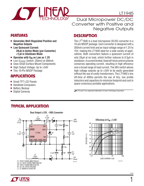
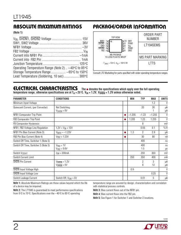
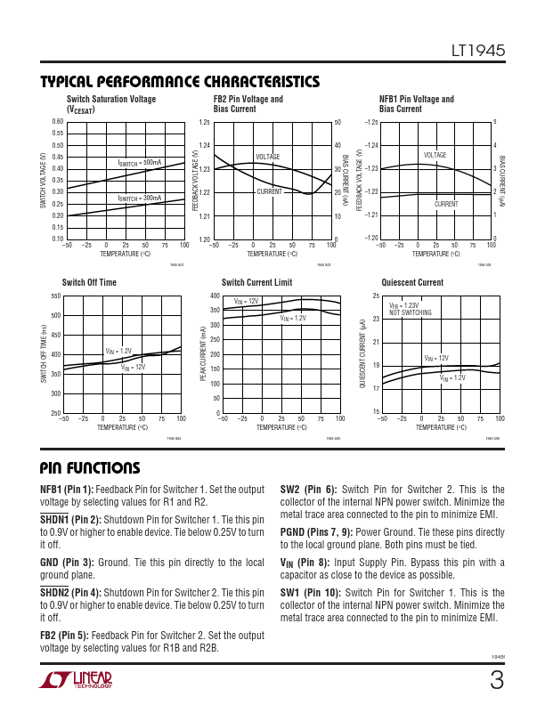
LT1945
ABSOLUTE AXI U RATI GS
(Note 1)
VIN, SHDN1, SHDN2 Voltage ................................... 15V
SW1, SW2 Voltage .................................................. 36V
NFB1 Voltage ........................................................... –3V
FB2 Voltage ...............................................................VIN
Current into NFB1 Pin ........................................... –1mA
Current into FB2 Pin .............................................. 1mA
Junction Temperature ........................................... 125°C
Operating Temperature Range (Note 2) .. – 40°C to 85°C
Storage Temperature Range ................. – 65°C to 150°C
Lead Temperature (Soldering, 10 sec).................. 300°C
UW U
PACKAGE/ORDER I FOR ATIO
NFB1 1
SHDN1 2
GND 3
SHDN2 4
FB2 5
TOP VIEW
10 SW1
9 PGND
8 VIN
7 PGND
6 SW2
MS PACKAGE
10-LEAD PLASTIC MSOP
TJMAX = 125°C, θJA = 160°C/W
ORDER PART
NUMBER
LT1945EMS
MS PART MARKING
LTTS
Consult LTC Marketing for parts specified with wider operating temperature ranges.
ELECTRICAL CHARACTERISTICS The q denotes the specifications which apply over the full operating
temperature range, otherwise specifications are at TA = 25°C. VIN = 1.2V, VSHDN = 1.2V unless otherwise noted.
PARAMETER
CONDITIONS
Minimum Input Voltage
Quiescent Current, (per Converter)
NFB1 Comparator Trip Point
Not Switching
VSHDN = 0V
FB2 Comparator Trip Point
FB Comparator Hysteresis
NFB1, FB2 Voltage Line Regulation
NFB1 Pin Bias Current (Note 3)
FB2 Pin Bias Current (Note 4)
Switch Off Time, Switcher 1 (Note 5)
1.2V < VIN < 12V
VNFB1 = –1.23V
VFB2 = 1.23V
Switch Off Time, Switcher 2 (Note 5)
Switch VCESAT
Switch Current Limit
VFB2 > 1V
VFB2 < 0.6V
ISW = 300mA
SHDN Pin Current
SHDN Input Voltage High
VSHDN = 1.2V
VSHDN = 5V
SHDN Input Voltage Low
Switch Leakage Current
Switch Off, VSW = 5V
Note 1: Absolute Maximum Ratings are those values beyond which the life
of a device may be impaired.
Note 2: The LT1945 is guaranteed to meet performance specifications
from 0°C to 70°C. Specifications over the – 40°C to 85°C operating
MIN
q –1.205
q 1.205
q 1.3
q
250
0.9
TYP
20
–1.23
1.23
8
0.05
2
30
400
400
1.5
250
350
2
8
0.01
MAX
1.2
30
1
–1.255
1.255
0.1
2.9
80
350
400
3
12
0.25
5
UNITS
V
µA
µA
V
V
mV
%/V
µA
nA
ns
ns
µs
mV
mA
µA
µA
V
V
µA
temperature range are assured by design, characterization and correlation
with statistical process controls.
Note 3: Bias current flows out of the NFB1 pin.
Note 4: Bias current flows into the FB2 pin.
Note 5: See Figure 1 for Switcher 1 and Switcher 2 locations.
1945f
2