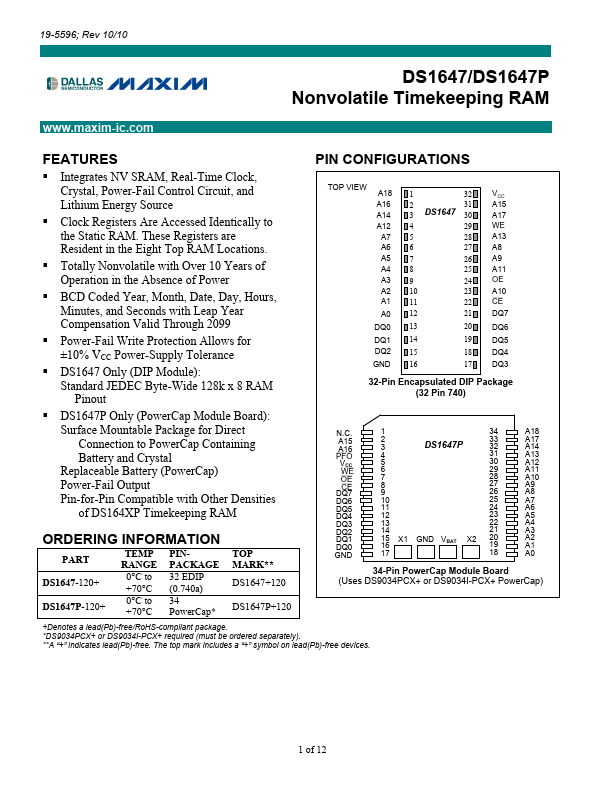
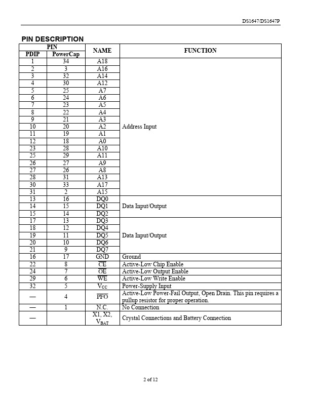
19-5596; Rev 10/10
www.maxim-ic.com
DS1647/DS1647P
Nonvolatile Timekeeping RAM
FEATURES
PIN CONFIGURATIONS
Integrates NV SRAM, Real-Time Clock,
Crystal, Power-Fail Control Circuit, and
Lithium Energy Source
Clock Registers Are Accessed Identically to
the Static RAM. These Registers are
Resident in the Eight Top RAM Locations.
Totally Nonvolatile with Over 10 Years of
Operation in the Absence of Power
BCD Coded Year, Month, Date, Day, Hours,
Minutes, and Seconds with Leap Year
Compensation Valid Through 2099
Power-Fail Write Protection Allows for
±10% VCC Power-Supply Tolerance
DS1647 Only (DIP Module):
Standard JEDEC Byte-Wide 128k x 8 RAM
Pinout
TOP VIEW
A18
A16
A14
A12
A7
A6
A5
A4
A3
A2
A1
A0
DQ0
DQ1
DQ2
GND
1 32
2 31
3 DS1647 30
4 29
5 28
6 27
7 26
8 25
9 24
10 23
11 22
12 21
13 20
14 19
15 18
16 17
VCC
A15
A17
WE
A13
A8
A9
A11
OE
A10
CE
DQ7
DQ6
DQ5
DQ4
DQ3
32-Pin Encapsulated DIP Package
(32 Pin 740)
DS1647P Only (PowerCap Module Board):
Surface Mountable Package for Direct
Connection to PowerCap Containing
Battery and Crystal
Replaceable Battery (PowerCap)
Power-Fail Output
Pin-for-Pin Compatible with Other Densities
of DS164XP Timekeeping RAM
ORDERING INFORMATION
PART
TEMP PIN-
RANGE PACKAGE
DS1647-120+
0°C to 32 EDIP
+70°C (0.740a)
DS1647P-120+
0°C to 34
+70°C PowerCap*
TOP
MARK**
DS1647+120
DS1647P+120
N.C.
A15
A16
PFO
VCC
WE
OE
CE
DQ7
DQ6
DQ5
DQ4
DQ3
DQ2
DQ1
DQ0
GND
1
2
3
DS1647P
4
5
6
7
8
9
10
11
12
13
14
15
16
X1
GND
VBAT
X2
17
34
33
32
31
30
29
28
27
26
25
24
23
22
21
20
19
18
A18
A17
A14
A13
A12
A11
A10
A9
A8
A7
A6
A5
A4
A3
A2
A1
A0
34-Pin PowerCap Module Board
(Uses DS9034PCX+ or DS9034I-PCX+ PowerCap)
+Denotes a lead(Pb)-free/RoHS-compliant package.
*DS9034PCX+ or DS9034I-PCX+ required (must be ordered separately).
**A “+” indicates lead(Pb)-free. The top mark includes a “+” symbol on lead(Pb)-free devices.
1 of 12