ML2340
ML2340 is Single Supply / Programmable 8-Bit D/A Converters manufactured by Micro Linear.
May 1997
ML2340- , ML2350-
- Single Supply, Programmable 8-Bit D/A Converters
GENERAL DESCRIPTION
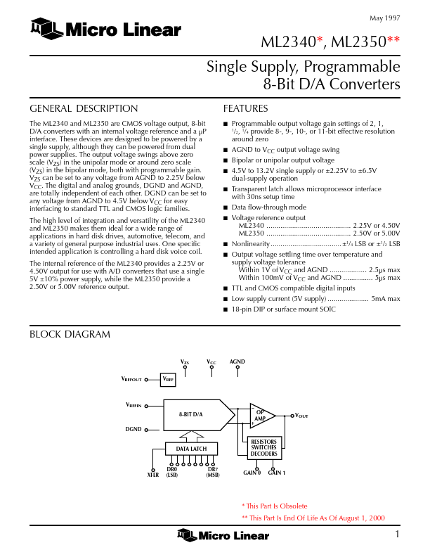
The ML2340 and ML2350 are CMOS voltage output, 8-bit D/A converters with an internal voltage reference and a µP interface. These devices are designed to be powered by a single supply, although they can be powered from dual power supplies. The output voltage swings above zero scale (VZS) in the unipolar mode or around zero scale (VZS) in the bipolar mode, both with programmable gain. VZS can be set to any voltage from AGND to 2.25V below VCC. The digital and analog grounds, DGND and AGND, are totally independent of each other. DGND can be set to any voltage from AGND to 4.5V below VCC for easy interfacing to standard TTL and CMOS logic families. The high level of integration and versatility of the ML2340 and ML2350 makes them ideal for a wide range of applications in hard disk drives, automotive, tele, and a variety of general purpose industrial uses. One specific intended application is controlling a hard disk voice coil. The internal reference of the ML2340 provides a 2.25V or 4.50V output for use with A/D converters that use a single 5V ±10% power supply, while the ML2350 provide a 2.50V or 5.00V reference output.
Features s
Programmable output voltage gain settings of 2, 1, 1 /2, 1/4 provide 8-, 9-, 10-, or 11-bit effective resolution around zero AGND to VCC output voltage swing Bipolar or unipolar output voltage 4.5V to 13.2V single supply or ±2.25V to ±6.5V dual-supply operation Transparent latch allows microprocessor interface with 30ns setup time Data flow-through mode Voltage reference output ML2340 ........................................... 2.25V or 4.50V ML2350 ........................................... 2.50V or 5.00V Nonlinearity .................................... ±1/4 LSB or ±1/2 LSB Output voltage settling time over temperature and supply voltage tolerance Within 1V of VCC and AGND ................... 2.5µs max Within 100m V of VCC and AGND...