MCP111
Features
- Ultra-Low Supply Current: 1.75 µA (Max.)
- Precision Monitoring Options Of:
- 1.90V, 2.32V, 2.63V, 2.90V, 2.93V, 3.08V, 4.38V and 4.63V
- Resets Microcontroller in a Power-Loss Event
- Active-Low VOUT Pin:
- MCP111 Active-Low, Open-Drain
- MCP112 Active-Low, Push-Pull
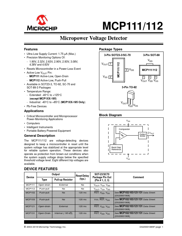
- Available in SOT23-3, TO-92, SC-70 and SOT-89-3 Packages
- Temperature Range:
- Extended: -40°C to +125°C
(except MCP1XX-195)
- Industrial: -40°C to +85°C (MCP1XX-195 Only)
- Pb-Free Devices
Applications
- Critical Microcontroller and Microprocessor Power-Monitoring Applications
- puters
- Intelligent Instruments
- Portable Battery-Powered Equipment
General Description
The MCP111/112 are voltage-detecting devices designed to keep a microcontroller in reset until the system voltage has stabilized at the appropriate level for reliable system operation. These devices also operate as protection from brown-out conditions when the system...