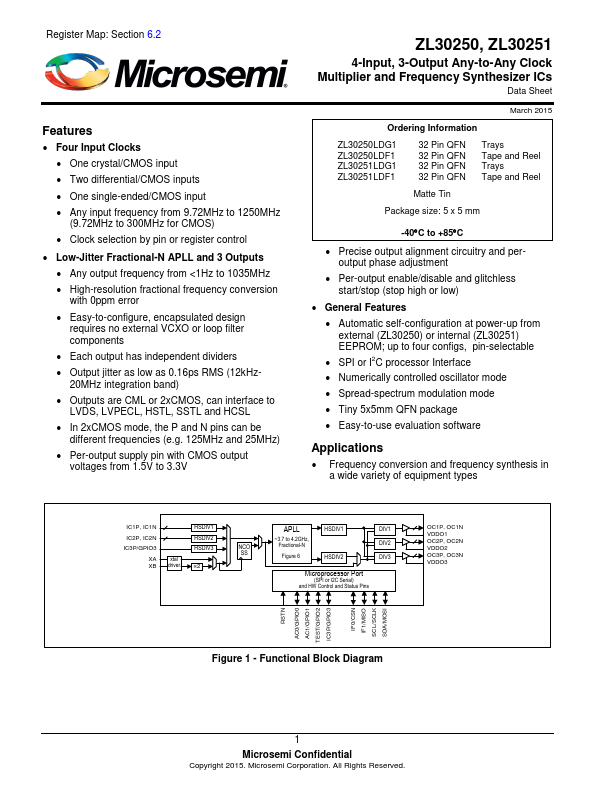
ZL30250 Overview
Register Map: Section.
ZL30250 Key Features
- Four Input Clocks
- One crystal/CMOS input
- Two differential/CMOS inputs
- One single-ended/CMOS input
- Any input frequency from 9.72MHz to 1250MHz (9.72MHz to 300MHz for CMOS)
- Clock selection by pin or register control
- Low-Jitter Fractional-N APLL and 3 Outputs
- Any output frequency from <1Hz to 1035MHz
- High-resolution fractional frequency conversion with 0ppm error
- Easy-to-configure, encapsulated design requires no external VCXO or loop filter ponents