ZL40241 - Ten LVCMOS Output Low Additive Jitter Fanout Buffer
Microsemi (now Microchip Technology)
General Description
6 Functional Description 8 Clock Inputs 8 Clock Outputs 11 Crystal Oscillator Input 11 Termination of unused inputs and outputs 12 Power Consumption 13 Power Supply Filtering 15 Device Control 15 AC and DC Electrical Characteristics 16 Absolute Maximum Ratings 16 Recommended Operating Cond
Key Features
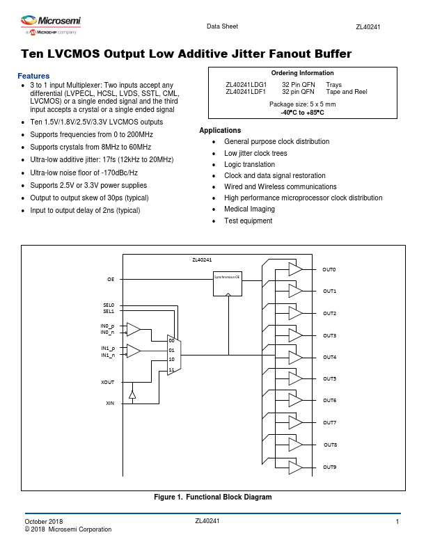
3 to 1 input Multiplexer: Two inputs accept any differential (LVPECL, HCSL, LVDS, SSTL, CML, LVCMOS) or a single ended signal and the third input accepts a crystal or a single ended signal.
Full PDF Text Transcription for ZL40241 (Reference)
Note: Below is a high-fidelity text extraction (approx. 800 characters) for
ZL40241. For precise diagrams, and layout, please refer to the original PDF.
Data Sheet ZL40241 Ten LVCMOS Output Low Additive Jitter Fanout Buffer Features • 3 to 1 input Multiplexer: Two inputs accept any differential (LVPECL, HCSL, LVDS, SSTL, ...
View more extracted text
plexer: Two inputs accept any differential (LVPECL, HCSL, LVDS, SSTL, CML, LVCMOS) or a single ended signal and the third input accepts a crystal or a single ended signal • Ten 1.5V/1.8V/2.5V/3.3V LVCMOS outputs • Supports frequencies from 0 to 200MHz • Supports crystals from 8MHz to 60MHz • Ultra-low additive jitter: 17fs (12kHz to 20MHz) • Ultra-low noise floor of -170dBc/Hz • Supports 2.5V or 3.
More Datasheets from Microsemi (now Microchip Technology)