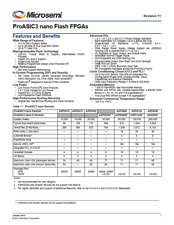
A3PN010 Key Features
- 10 k to 250 k System Gates
- Up to 36 kbits of True Dual-Port SRAM
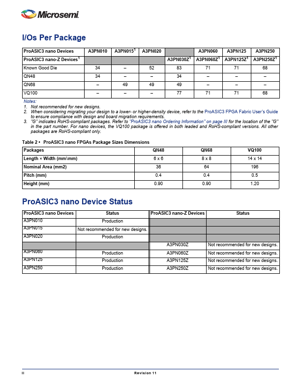
- Up to 71 User I/Os
- 1.5 V, 1.8 V, 2.5 V, and 3.3 V Mixed-Voltage Operation
- Bank-Selectable I/O Voltages-up to 4 Banks per Chip
- Single-Ended I/O Standards: LVTTL, LVCMOS 3.3 V / 2.5 V / 1.8 V / 1.5 V
- Wide Range Power Supply Voltage Support per JESD8-B, Allowing I/Os to Operate from 2.7 V to 3.6 V
- I/O Registers on Input, Output, and Enable Paths
- Selectable Schmitt Trigger Inputs
- Hot-Swappable and Cold-Sparing I/Os