M62015L
M62015L is LOW POWER 2 OUTPUT SYSTEM RESET IC manufactured by Mitsubishi Electric.
MITSUBISHI <Dig./Ana.INTERFACE>
M62015L,FP M62016L,FP
LOW POWER 2 OUTPUT SYSTEM RESET IC DESCRIPTION PIN CONFIGURATION (TOP VIEW)
The M62015, M62016 are semiconductor integrated circuits whose optimum use is for the detection of the rise and fall in the power supply to a microputer system in order to reset or release the microputer system. The M62015, M62016 carry out voltage detection in 2 steps and have 2 output pins. As Bi-CMOS process and low power dissipating circuits are employed, they output optimum signals through each output pin to a system that requires RAM backup. These ICs also support the backup mode of Mitsubishi microputer the M16C.
5 4 3 2 1
VCC Cd RESET INT GND
Outline 5P5T RESET 1 Cd 2 VCC 3 NC 4 INT GND NC NC
Features
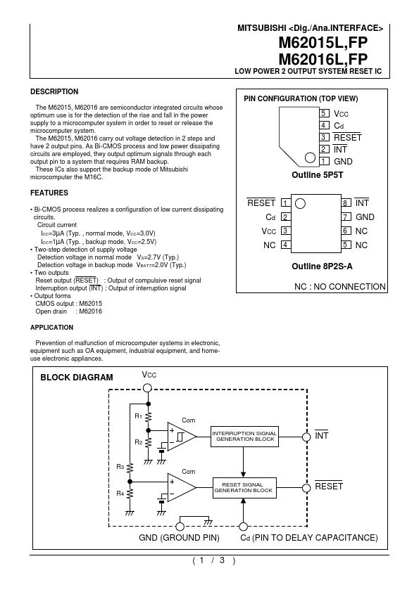
- Bi-CMOS process realizes a configuration of low current dissipating circuits. Circuit current ICC=3µA (Typ. , normal mode, VCC=3.0V) ICC=1µA (Typ. , backup mode, VCC=2.5V)
- Two-step detection of supply voltage Detection voltage in normal mode VS=2.7V (Typ.) Detection voltage in backup mode VBATT=2.0V (Typ.)
- Two outputs Reset output (RESET) : Output of pulsive reset signal Interruption output (INT) : Output of interruption signal
- Output forms CMOS output : M62015 Open drain : M62016 APPLICATION Prevention of malfunction of microputer systems in electronic, equipment such as OA equipment, industrial equipment, and homeuse electronic appliances.
8 7 6 5
Outline 8P2S-A NC : NO CONNECTION
BLOCK DIAGRAM
R1
INTERRUPTION SIGNAL GENERATION BLOCK
R2
R3
RESET SIGNAL GENERATION BLOCK
RESET
R4
GND (GROUND PIN) ( 1 / 3 )
Cd (PIN TO DELAY CAPACITANCE)
MITSUBISHI <Dig./Ana.INTERFACE>
M62015L,FP / M62016L,FP
LOW POWER 2 OUTPUT SYSTEM RESET...