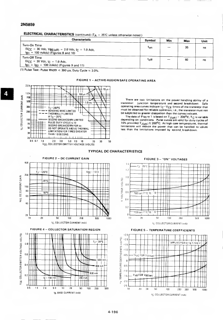
The following content is an automatically extracted verbatim text
from the original manufacturer datasheet and is provided for reference purposes only.
View original datasheet text
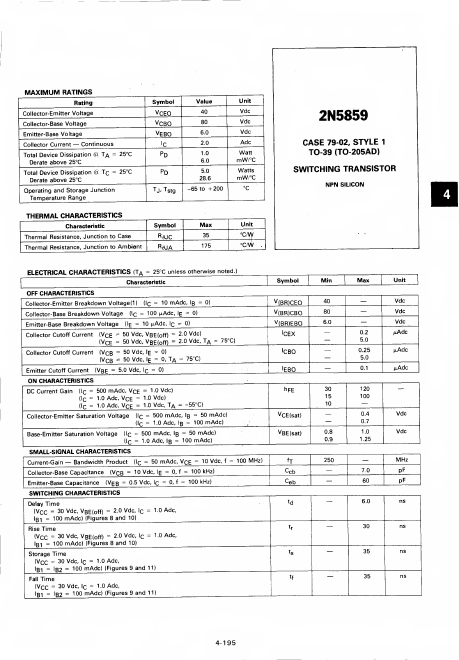
)
MAXIMUM RATINGS
Rating
Collector-Emitter Voltage
Collector-Base Voltage
Emitter-Base Voltage
—Collector Current Continuous
Total Device Dissipation (S TA = 25°C
Derate above 25°C Total Device Dissipation (a Tq = 25°C
Derate above 25°C
Operating and Storage Junction Temperature Range
Symbol VCEO VCBO VEBO
"c
PD
PD
Tj. T stg
Value 40 80 6.0 2.0
1.0 6.0 5.0 28.6
-65 to + 200
Unit Vdc Vdc Vdc Adc Watt
mW/°C Watts mW/°C
°C
THERMAL CHARACTERISTICS
Characteristic Thermal Resistance, Junction to Case
Thermal Resistance, Junction to Ambient
Symbol R&jc R&JA
Max
35 175
Unit °C/W °C/W .
2N5859
CASE 79-02, STYLE 1
TO-39 (TO-205AD)
SWITCHING TRANSISTOR
NPN SILICON
ELECTRICAL CHARACTERISTICS (TA = 25°C unless otherwise noted.