MC74AC299 Overview
Key Features
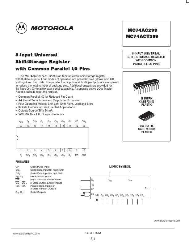
- Common Parallel I/O for Reduced Pin Count Additional Serial Inputs and Outputs for Expansion Four Operating Modes: Shift Left, Shift Right, Load and Store 3-State Outputs for Bus-Oriented Applications Outputs Source/Sink 24 mA ′ACT299 Has TTL Compatible Inputs
- I/O7 Q0, Q7 Clock Pulse Input Serial Data Input for Right Shift Serial Data Input for Left Shift Mode Select Inputs Asynchronous Master Reset 3-State Output Enable Inputs Parallel Data Inputs or 3-State Parallel Outputs Serial Outputs