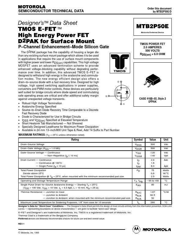
Datasheet4U Logo Datasheet4U.com

MTB2P50E - TMOS POWER FET

Features

  • sistance is difficult to measure and, consequently, is not specified. The resistive switching time variation versus gate resistance (Figure 9) shows how typical switching performance is affected by the parasitic circuit elements. If the parasitics were not present, the slope of the curves would maintain a value of unity regardless of the switching speed. The circuit used to obtain the data is constructed to minimize common inductance in the drain and gate circuit loops and is believed readily ac.

📥 Download Datasheet

Full PDF Text Transcription (Reference)

The following content is an automatically extracted verbatim text from the original manufacturer datasheet and is provided for reference purposes only.

View original datasheet text
MOTOROLA SEMICONDUCTOR TECHNICAL DATA Order this document by MTB2P50E/D ™ Data Sheet TMOS E-FET.™ High Energy Power FET D2PAK for Surface Mount Designer's MTB2P50E Motorola Preferred Device P–Channel Enhancement–Mode Silicon Gate The D2PAK package has the capability of housing a larger die than any existing surface mount package which allows it to be used in applications that require the use of surface mount components with higher power and lower RDS(on) capabilities. This high voltage MOSFET uses an advanced termination scheme to provide enhanced voltage–blocking capability without degrading performance over time. In addition, this advanced TMOS E–FET is designed to withstand high energy in the avalanche and commutation modes.
Published: |