MTD6P10E Overview
Key Specifications
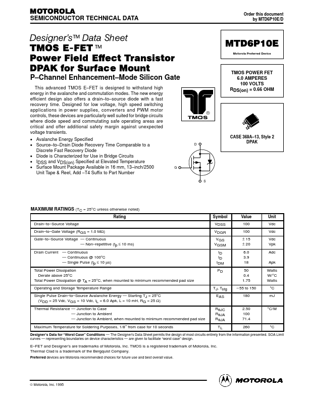
Package: TO-252-3
Mount Type: Surface Mount
Pins: 3
Max Operating Temp: 150 °C
Key Features
- Channel Enhancement
- Mode Silicon Gate
| Part | MTD6P10E |
|---|---|
| Description | TMOS POWER FET 6.0 AMPERES 100 VOLTS RDS(on) = 0.66 OHM |
| Manufacturer | Motorola Semiconductor |
| Size | 261.77 KB |
Package: TO-252-3
Mount Type: Surface Mount
Pins: 3
Max Operating Temp: 150 °C
| Seller | Inventory | Price Breaks | Buy |
|---|---|---|---|
| Microchip USA | 236 | 600+ : 4.2446722 USD 1000+ : 4.2315308 USD 10000+ : 4.2183894 USD |
View Offer |
| Win Source | 4440 | 19+ : 3.1287 USD 45+ : 2.5673 USD 70+ : 2.4869 USD 96+ : 2.4067 USD |
View Offer |
| Part Number | Manufacturer | Description |
|---|---|---|
| MTD6P10E | onsemi | Power MOSFET |