MTP23P06V Overview
Key Specifications
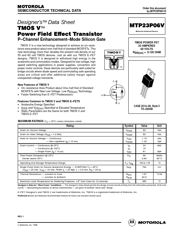
Package: TO-220AB
Mount Type: Through Hole
Pins: 3
Max Operating Temp: 175 °C
Key Features
- On–resistance Area Product about One–half that of Standard MOSFETs with New Low Voltage, Low RDS(on) Technology
- Faster Switching than E–FET Predecessors Features Common to TMOS V and TMOS E–FETS
- Avalanche Energy Specified
- IDSS and VDS(on) Specified at Elevated Temperature
- Continuous Gate–to–Source Voltage