Datasheet4U Logo Datasheet4U.com

MRF7S18170HSR3 - RF Power Field Effect Transistors

Download the MRF7S18170HSR3 datasheet PDF. This datasheet also covers the MRF7S18170H variant, as both devices belong to the same rf power field effect transistors family and are provided as variant models within a single manufacturer datasheet.

Description

0.8 pF Chip Capacitor 6.8 pF Chip Capacitors 100 pF Chip Capacitor 100 nF Chip Capacitor 5.6 pF Chip Capacitors 10 μF Chip Capacitors 470 μF, 63 V Electrolytic Capacitor, Radial 0.5 pF Chip Capacitor 0.2 pF Chip Capacitors 4.7 pF Chip Capacitors 2 pF Chip Capacitor 0.3 pF Chip Capacitor 10 W, 1/4 W

Features

  • 100% PAR Tested for Guaranteed Output Power Capability.
  • Characterized with Series Equivalent Large - Signal Impedance Parameters.
  • Internally Matched for Ease of Use.
  • Integrated ESD Protection.
  • Greater Negative Gate - Source Voltage Range for Improved Class C Operation.
  • Designed for Digital Predistortion Error Correction Systems.
  • RoHS Compliant.
  • In Tape and Reel. R3 Suffix = 250 Units per 56 mm, 13 inch Reel. MRF7S18170HR3.

📥 Download Datasheet

Note: The manufacturer provides a single datasheet file (MRF7S18170H_MotorolaSemiconductor.pdf) that lists specifications for multiple related part numbers.

Datasheet Details

Part number MRF7S18170HSR3
Manufacturer Motorola Semiconductor
File Size 520.47 KB
Description RF Power Field Effect Transistors
Datasheet download datasheet MRF7S18170HSR3 Datasheet

Full PDF Text Transcription (Reference)

The following content is an automatically extracted verbatim text from the original manufacturer datasheet and is provided for reference purposes only.

View original datasheet text
www.DataSheet4U.com 
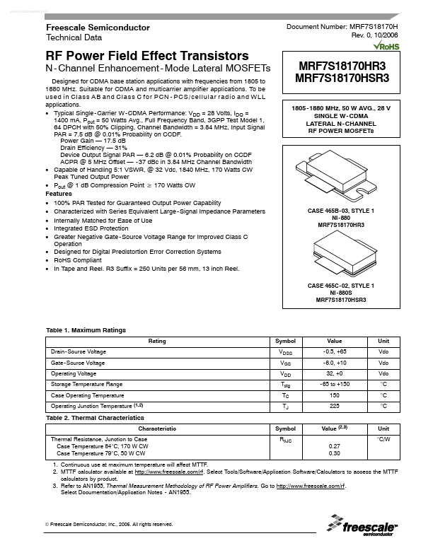
Freescale Semiconductor Technical Data Document Number: MRF7S18170H Rev. 0, 10/2006 RF Power Field Effect Transistors N - Channel Enhancement - Mode Lateral MOSFETs Designed for CDMA base station applications with frequencies from 1805 to 1880 MHz. Suitable for CDMA and multicarrier amplifier applications. To be used in Class AB and Class C for PCN - PCS/cellular radio and WLL applications. • Typical Single - Carrier W - CDMA Performance: VDD = 28 Volts, IDQ = 1400 mA, Pout = 50 Watts Avg., Full Frequency Band, 3GPP Test Model 1, 64 DPCH with 50% Clipping, Channel Bandwidth = 3.84 MHz, Input Signal PAR = 7.5 dB @ 0.01% Probability on CCDF. Power Gain — 17.5 dB Drain Efficiency — 31% Device Output Signal PAR — 6.2 dB @ 0.
Published: |