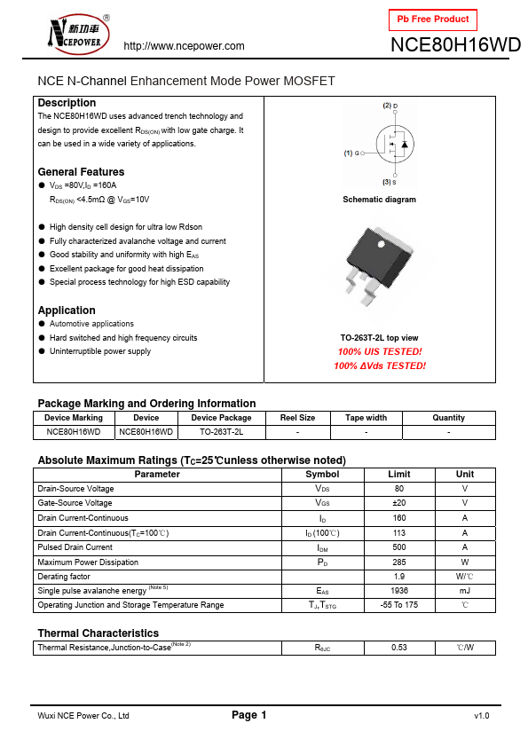
http://www.ncepower.com
Electrical Characteristics (TC=25℃unless otherwise noted)
Parameter
Symbol
Condition
Off Characteristics
Drain-Source Breakdown Voltage
Zero Gate Voltage Drain Current
Gate-Body Leakage Current
On Characteristics (Note 3)
BVDSS
IDSS
IGSS
VGS=0V ID=250μA
VDS=80V,VGS=0V
VGS=±20V,VDS=0V
Gate Threshold Voltage
Drain-Source On-State Resistance
Forward Transconductance
Dynamic Characteristics (Note4)
VGS(th)
RDS(ON)
gFS
VDS=VGS,ID=250μA
VGS=10V, ID=20A
VDS=5V,ID=20A
Input Capacitance
Output Capacitance
Reverse Transfer Capacitance
Switching Characteristics (Note 4)
Clss
Coss
Crss
VDS=25V,VGS=0V,
F=1.0MHz
Turn-on Delay Time
Turn-on Rise Time
Turn-Off Delay Time
Turn-Off Fall Time
Total Gate Charge
Gate-Source Charge
Gate-Drain Charge
td(on)
tr
td(off)
tf
Qg
Qgs
Qgd
VDD=40V,RL=15Ω
VGS=10V,RG=2.5Ω
VDS=40V,ID=20A,
VGS=10V
Drain-Source Diode Characteristics
Diode Forward Voltage (Note 3)
Diode Forward Current (Note 2)
Reverse Recovery Time
Reverse Recovery Charge
VSD VGS=0V,IS=40A
IS
trr TJ = 25°C, IF = 20A
Qrr di/dt = 500A/μs(Note3)
Pb Free Product
NCE80H16WD
Min Typ Max Unit
80 88
-
--
1
- - ±100
V
μA
nA
23
- 3.5
60 -
4
4.5
-
V
mΩ
S
- 6500
- 810
- 310
-
-
-
PF
PF
PF
- 31.5
- 33
- 46
- 17.5
- 130
- 36
- 46
-
-
-
-
nS
nS
nS
nS
nC
nC
nC
- 1.2
- - 160
- 51
-
- 61
-
V
A
nS
nC
Notes:
1. Repetitive Rating: Pulse width limited by maximum junction temperature.
2. Surface Mounted on FR4 Board, t ≤ 10 sec.
3. Pulse Test: Pulse Width ≤ 300μs, Duty Cycle ≤ 2%.
4. Guaranteed by design, not subject to production
5. EAS condition:Tj=25℃,VDD=40V,VG=10V,L=0.5mH,Rg=25Ω
Wuxi NCE Power Co., Ltd
Page 2
v1.0