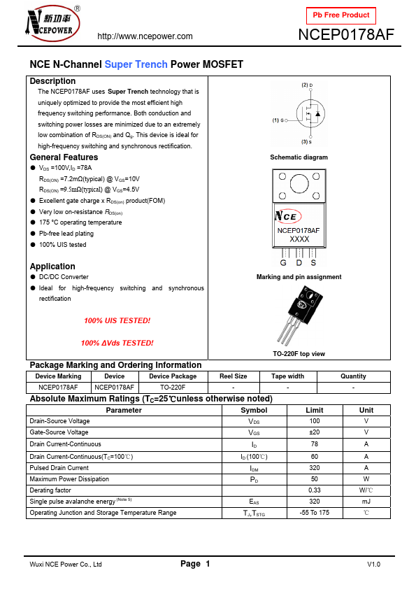
http://www.ncepower.com
Thermal Characteristic
Thermal Resistance,Junction-to-Case(Note 2)
RθJC
Electrical Characteristics (TC=25℃unless otherwise noted)
Parameter
Symbol
Condition
Off Characteristics
Drain-Source Breakdown Voltage
Zero Gate Voltage Drain Current
Gate-Body Leakage Current
On Characteristics (Note 3)
BVDSS
IDSS
IGSS
VGS=0V ID=250μA
VDS=100V,VGS=0V
VGS=±20V,VDS=0V
Gate Threshold Voltage
Drain-Source On-State Resistance
Forward Transconductance
Dynamic Characteristics (Note4)
VGS(th)
RDS(ON)
gFS
VDS=VGS,ID=250μA
VGS=10V, ID=39A
VGS=4.5V, ID=39A
VDS=10V,ID=39A
Input Capacitance
Output Capacitance
Reverse Transfer Capacitance
Switching Characteristics (Note 4)
Clss
Coss
Crss
VDS=50V,VGS=0V,
F=1.0MHz
Turn-on Delay Time
Turn-on Rise Time
Turn-Off Delay Time
Turn-Off Fall Time
Total Gate Charge
Gate-Source Charge
Gate-Drain Charge
td(on)
tr
td(off)
tf
Qg
Qgs
Qgd
VDD=50V,ID=39A
VGS=10V,RG=4.7Ω
VDS=50V,ID=39A,
VGS=10V
Drain-Source Diode Characteristics
Diode Forward Voltage (Note 3)
Diode Forward Current (Note 2)
Reverse Recovery Time
Reverse Recovery Charge
VSD VGS=0V,IS=78A
IS
trr TJ = 25°C, IF = IS
Qrr di/dt = 100A/μs(Note3)
Pb Free Product
NCEP0178AF
3 ℃/W
Min Typ Max Unit
100
--
--
-
1
±100
V
μA
nA
1.2 1.7
- 7.2
- 9.5
40 -
2.2
8.5
12
-
V
mΩ
mΩ
S
- 4200 5480
- 354 425
- 23
30
PF
PF
PF
- 15
- 10
- 41
-6
- 65
- 15.3
-9
-
-
-
-
nS
nS
nS
nS
nC
nC
nC
- 1.2
--
78
- 101
- 193
V
A
nS
nC
Notes:
1. Repetitive Rating: Pulse width limited by maximum junction temperature.
2. Surface Mounted on FR4 Board, t ≤ 10 sec.
3. Pulse Test: Pulse Width ≤ 300μs, Duty Cycle ≤ 2%.
4. Guaranteed by design, not subject to production
5. EAS condition : Tj=25℃,VDD=50V,VG=10V,L=0.5mH,Rg=25Ω
Wuxi NCE Power Co., Ltd
Page 2
V1.0