J132
FEATURES
- Gate drive available at logic level (VGS =
- 4 V)
- High current control available in small dimension due to low RDS(on) (≅ 0.25 Ω)
- 2SJ132-Z is a lead process product and is deal for mounting a hybrid IC.
QUALITY GRADES
- Standard
Please refer to “Quality Grades on NEC Semiconductor Devices” (Document No. C11531E) published by NEC Corporation to know the specification of quality grade on the devices and its remended applications.
ABSOLUTE MAXIMUM RATINGS (Ta = 25°C)
Parameter
Symbol
Conditions
Drain to source voltage
VDSS
VGS = 0
Gate to source voltage
VGSS
VDS = 0
Drain current (DC)
ID(DC)
TC = 25°C
Drain current (pulse)
ID(pulse)
PW ≤ 300 µs duty cycle ≤ 10 %
Total power dissipation
PT TC = 25°C
Total power dissipation
PT Ta = 25°C
Channel temperature
Tch
Storage temperature
Tstg
- Printing board mounted
- - 7.5 cm2 × 0.7 mm ceramic board mounted
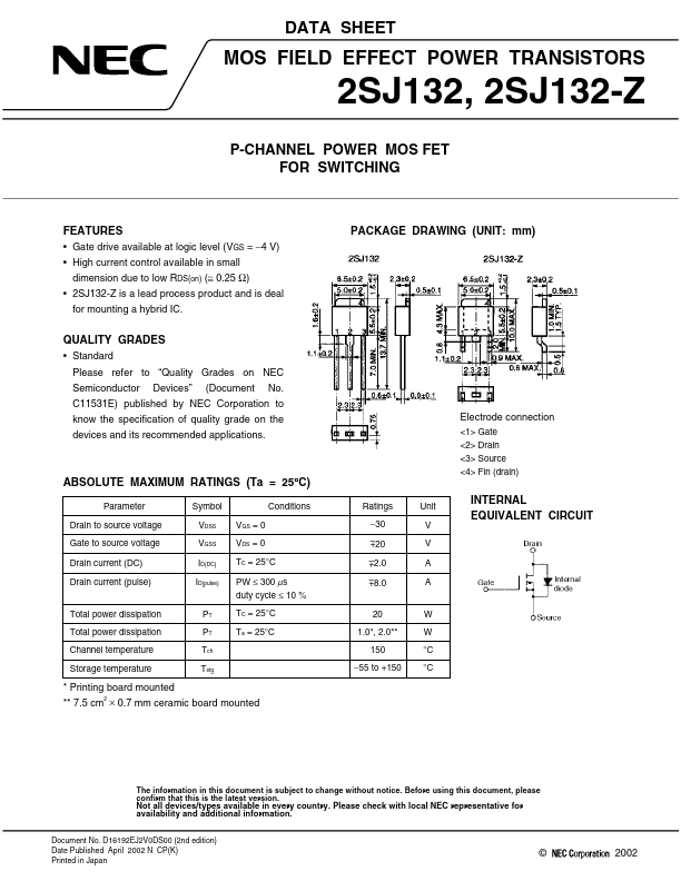
PACKAGE DRAWING (UNIT: mm)
Ratings
- 30 +- 20 +- 2.0 +- 8.0
Electrode connection <1> Gate <2> Drain <3>...