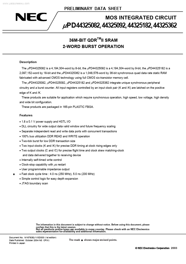
UPD44325362 Overview
Key Specifications
Package: FBGA
Pins: 165
Operating Voltage: 1.8 V
Max Voltage (typical range): 1.9 V
Description
The µPD44325082 is a 4,194,304-word by 8-bit, the µPD44325092 is a 4,194,304-word by 9-bit, the µPD44325182 is a 2,097,152-word by 18-bit and the µPD44325362 is a 1,048,576-word by 36-bit synchronous quad data rate static RAM fabricated with advanced CMOS technology using full CMOS six-transistor memory cell. The µPD44325082, µPD44325092, µPD44325182 and µPD44325362 integrate unique synchronous peripheral circuitry and a burst counter.
Key Features
- 1.8 ± 0.1 V power supply and HSTL I/O
- DLL circuitry for wide output data valid window and future frequency scaling
- Separate independent read and write data ports with concurrent transactions
- 100% bus utilization DDR READ and WRITE operation
- Two-tick burst for low DDR transaction size
- Two input clocks (K and /K) for precise DDR timing at clock rising edges only
- Two output clocks (C and /C) for precise flight time and clock skew matching-clock and data delivered together to receiving device
- Internally self-timed write control
- Clock-stop capability with µs restart
- User programmable impedance output

