UPD8748 Description
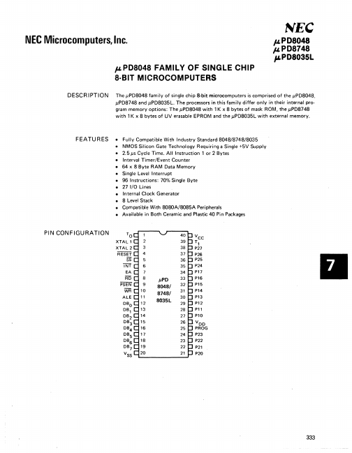
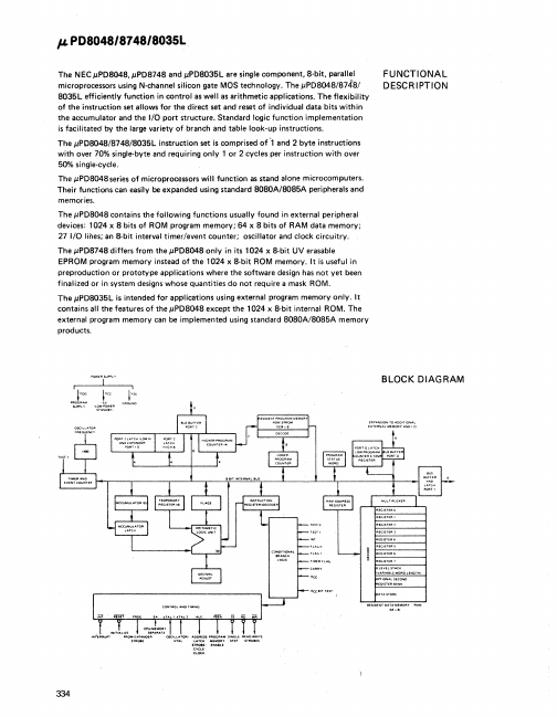
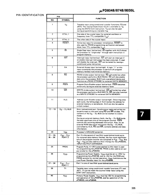
BLOCK DIAGRAM 334 "cC'''UST IV,",fU",BU WOAO LEfIrIGTHI PIN IDENTIFICATION PIN NO. SYMBOL 1 TO 2 XTALI 3 XTAL2 4 RESET.
UPD8748 is SINGLE CHIP 8-BIT MICROCOMPUTERS manufactured by NEC.
| Manufacturer | Part Number | Description |
|---|---|---|
| UPD8748H | (UPD8748H / UPD8749H) 8-Bit NMOS Microcomputer |
BLOCK DIAGRAM 334 "cC'''UST IV,",fU",BU WOAO LEfIrIGTHI PIN IDENTIFICATION PIN NO. SYMBOL 1 TO 2 XTALI 3 XTAL2 4 RESET.