Download the P2503HVG datasheet PDF.
This datasheet also covers the P2503HVG-NIKO variant, as both devices belong to the same dual n-channel fet family and are provided as variant models within a single manufacturer datasheet.
Full PDF Text Transcription for P2503HVG (Reference)
Note: Below is a high-fidelity text extraction (approx. 800 characters) for
P2503HVG. For precise diagrams, and layout, please refer to the original PDF.
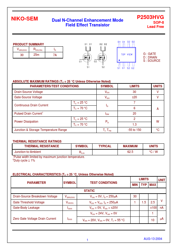
NIKO-SEM Dual N-Channel Enhancement Mode Field Effect Transistor P2503HVG SOP-8 Lead Free PRODUCT SUMMARY V(BR)DSS RDS(ON) 30 25m ID 7A G : GATE D : DRAIN S : SOURCE ABSO...
View more extracted text
MMARY V(BR)DSS RDS(ON) 30 25m ID 7A G : GATE D : DRAIN S : SOURCE ABSOLUTE MAXIMUM RATINGS (TC = 25 °C Unless Otherwise Noted) PARAMETERS/TEST CONDITIONS SYMBOL Drain-Source Voltage Gate-Source Voltage Continuous Drain Current Pulsed Drain Current1 Power Dissipation Junction & Storage Temperature Range TC = 25 °C TC = 70 °C TC = 25 °C TC = 70 °C VDS VGS ID IDM PD Tj, Tstg THERMAL RESISTANCE RATINGS THERMAL RESISTANCE SYMBOL Junction-to-Ambient RθJA 1Pulse width limited by maximum junction temperature. 2Duty cycle ≤ 1% TYPICAL LIMITS 30 ±20 7 6 20 2 1.3 -55 to 150 UNITS V V A W °C MAXIMUM 62.